Semiconductor test device for conducting an operation test in parallel on many chips in a wafer test and semiconductor test method

Inactive Publication Date: 2005-01-18
RENESAS ELECTRONICS CORP
View PDF6 Cites 28 Cited by
  • Summary
  • Abstract
  • Description
  • Claims
  • Application Information

AI Technical Summary

Benefits of technology

A major advantage of the invention is that the operation test is conducted simultaneously in parallel on the plurality of chips on the test target wafer through the first wafer contactor so that many chips on the common wafer can be simultaneously tested in parallel while suppressing increase in layout area of the chips to be tested.
is that the operation test is conducted simultaneously in parallel on the plurality of chips on the test target wafer through the first wafer contactor so that many chips on the common wafer can be simultaneously tested in parallel while suppressing increase in layout area of the chips to be tested.
According to another aspect of the invention, a semiconductor test method of conducting an operation test on a wafer level includes the steps of electrically coupling first and second wafers together through a wafer contactor; producing a plurality of test signals for conducting the operation test on a plurality of first chips formed on the first wafer by a plurality of second chips formed on the second wafer corresponding to the plurality of first chips, respectively; transmitting the plurality of test signals from the second wafer to the first wafer via the wafer contactor; and transmitting a plurality of test data issued from the plurality of first chips to the second wafer from the first wafer through the wafer contactor in response to the plurality of test signals.
Accordingly, the operation test can be conducted on each chip on the first wafer by transmitting the signal produced by each chip on the second wafer via the wafer contactor. Therefore, increase in layout area of the chip to be tested can be suppressed, and further the electrical coupling between the wafers allows the simultaneous and parallel test of the many chips on the same wafer.
According to still another aspect of the invention, a semiconductor device includes a plurality of memory mats and an internal test circuit.
The plurality of memory mats operate in accordance with a plurality of independent address signals, respectively. Each memory mat includes a regular memory array having a plurality of memory cells arranged in rows and columns. The internal test circuit conducts an operation test on the plurality of memory mats. The internal test circuit includes a test pattern generating portion for generating a test signal to be supplied to the plurality of memory mats for conducting the operation test, a redundant repair determining portion for detecting a defective memory cell in the regular memory array in each memory mat based on test data issued from each memory mat in response to the test signal, and a defective address storing portion for storing a defective address indicative of the defective memory cell.

Problems solved by technology

(1) Due to a structure of a probe of a probe card for bringing a chip to be tested into electrical contact with a semiconductor test device, It is difficult to perform simultaneous contact with many chips.
(2) Since there are restrictions on numbers of power supplies on the semiconductor test device side, clock drivers and signals, it is difficult, e.g., to generate signals for simultaneously testing many chips. Further, due to the structure of the probe card, it is difficult to arrange many signal lines. This also restricts the simultaneously testable number.
However, it is impossible to overcome the foregoing problem (2) only by the technology of the wafer test using the wafer contactor described above, and it is difficult to improve the simultaneously testable number.
However, each chip must include a circuit having the BIST function, resulting in increase in chip area and cost.
Therefore, the BIST system containing such test circuits further increases the required chip area.
Therefore, internal arrangement of the test circuits results in a waste of structure.

Method used


Image

  • Semiconductor test device for conducting an operation test in parallel on many chips in a wafer test and semiconductor test method
  • Semiconductor test device for conducting an operation test in parallel on many chips in a wafer test and semiconductor test method
  • Semiconductor test device for conducting an operation test in parallel on many chips in a wafer test and semiconductor test method

Examples


first embodiment

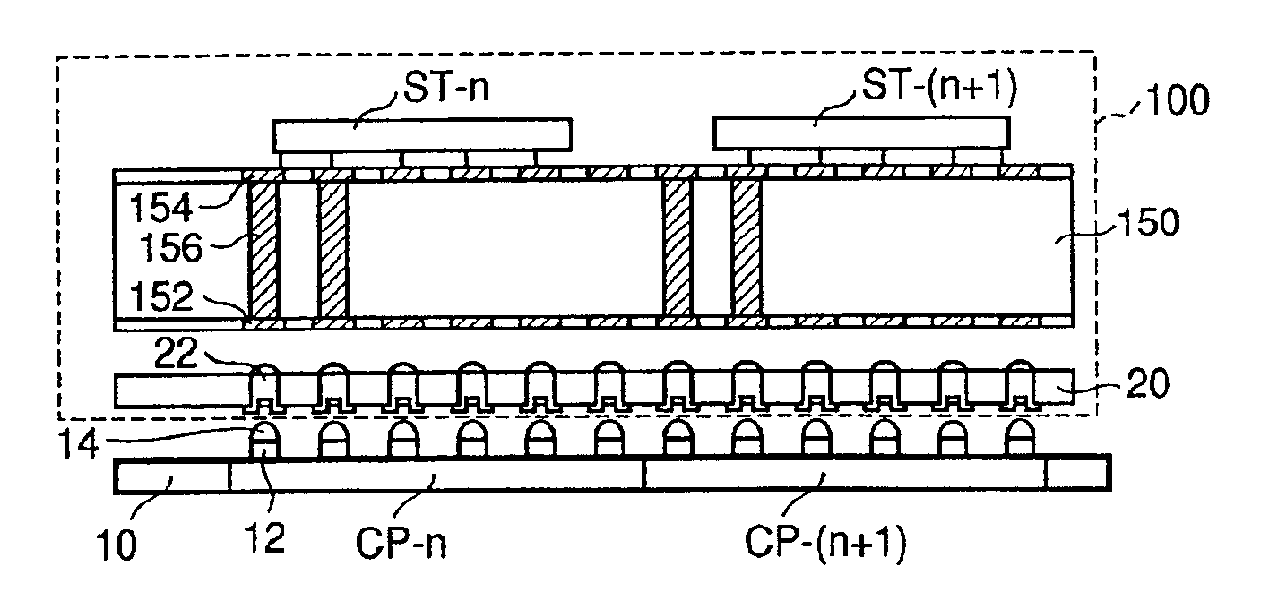
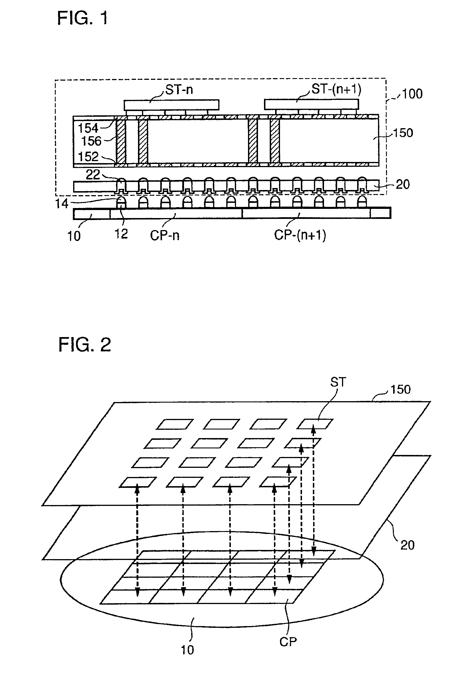
Referring to FIG. 1, a test target wafer 10 to be tested has a plurality of chips CP. FIG. 1 shows chips CP-n and CP-(n+1) in the nth (n: natural number) and (n+1)th positions among these plurality of chips CP. An electrode pad 12 allowing input / output of an electrical signal is arranged on each chip, and a bump 14 is also provided for achieving a good electrical contact between electrode pad 12 and an external system.

Semiconductor test device 100 according to the first embodiment includes a wafer contactor 20 and a test board 150. Wafer contactor 20 includes a plurality of contact terminals 22 provided corresponding to the plurality of bumps 14, respectively. Each contact terminal 22 can be in electrical contact with bump 14, and thereby can be electrically coupled to corresponding electrode pad 12 on chip CP simultaneously. Test target wafer 10 including bumps 14 and wafer contactor 20 are similar to those shown in FIGS. 23 and 24, and therefore description thereof is not repeated...

second embodiment

As a second embodiment of the invention, description will now be given on a structure for performing a wafer test, in which a test wafer which carries a circuit having a test function is used corresponding to test target wafer 10, and is connected thereto via a wafer contactor for performing the wafer test.

Referring to FIG. 4, semiconductor test device 200 according to the second embodiment differs from semiconductor test device 100 shown in FIG. 1 in that a test wafer 210 and a wafer contactor 220 are further employed. Test wafer 210 has a plurality of chips SCP corresponding to the plurality of chips CP on test target wafer 10, respectively. In semiconductor test device 200, the circuit for performing the self-test corresponding to the BIST function is not arranged on the test board 150, but is arranged on test wafer 210. On test wafer 210, electrode pads 212 and 214 are arranged similarly to test target wafer 10.

Wafer contactor 220 is provided for ensuring electrical contact betw...

third embodiment

As a third embodiment, description will be given on a structure, in which a portion of components of the self-test circuit is mounted on the chip to be tested.

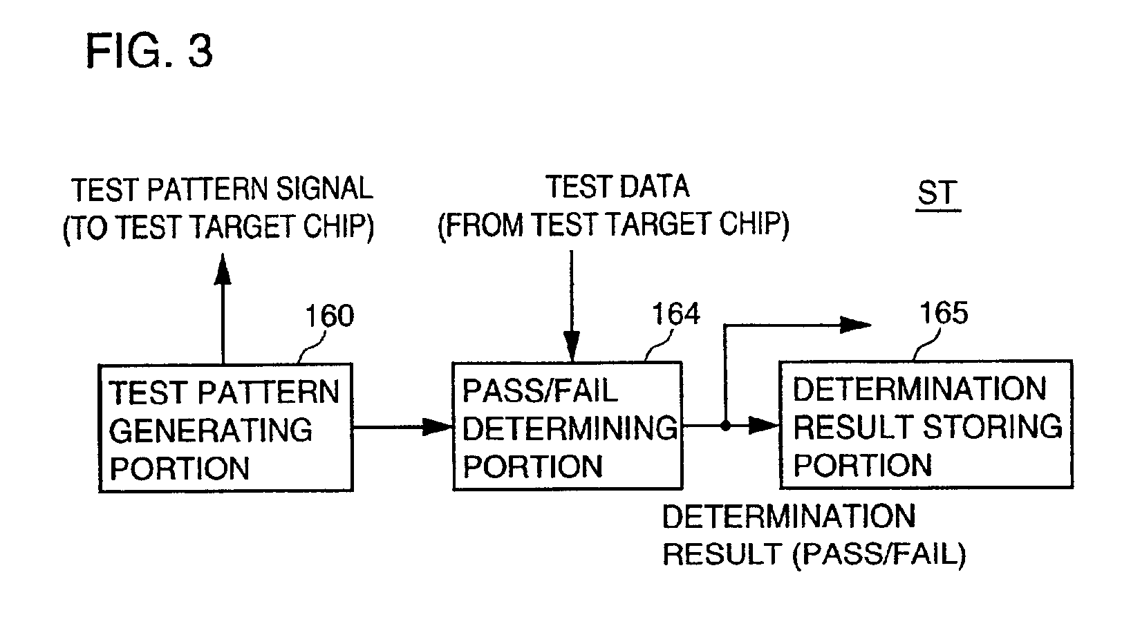
Referring to FIG. 9, self-test circuit STR further includes a redundant repair determining portion 166, which performs determination relating to redundant repair based on the test data, in addition to test pattern generating portion 160 for generating a test pattern signal and PASS / FAIL determining portion 164 receiving test data issued from the test target in response to the test pattern signal. Redundant repair determining portion 166 determines presence / absence of a defective portion, and analyses an address of the defective portion based on the test data. Redundant repair determining portion 166 issues redundant repair data including a defective address indicative of the defective portion. Although not shown, the structure may be additionally provided with a portion for storing redundant repair data.

The test target in whic...


PUM


Abstract

A plurality of test target chips on a test target wafer are simultaneously and electrically coupled to a plurality of chips on a test wafer via a wafer contactor. Each chip on the test wafer has a test circuit for conducting an operation test on each chip on the test target wafer. Since the test circuit is in a one-to-one relationship with respect to the test target chip, and is arranged on the test wafer other than the test target wafer, the many chips can be simultaneously tested in parallel during the wafer test without increasing an area of the test target chips.

Description

BACKGROUND OF THE INVENTION1. Field of the InventionThe present invention relates to a semiconductor test device, and particularly a semiconductor test device for evaluating an operation of a semiconductor device in a state of wafer (which will also be referred to as a “wafer level” hereinafter) as well as a semiconductor test method using the semiconductor test device.2. Description of the Background ArtIn accordance with development of a wafer level CSP (Chip Size Package) technology for processing package steps in the state of wafer, a semiconductor test device which conducts an operation test on a semiconductor device on the wafer level, which will be merely referred to as a “wafer test” hereinafter) has been of increasing importance. In a conventional semiconductor test device for the wafer test, the number of chips which can be simultaneously subjected to a parallel test, i.e., a simultaneously testable number is restricted primarily due to the following two problems.(1) Due t...

Claims


Application Information

Patent Timeline
IPC IPC(8): G11C29/48G11C29/04G01R1/073H01L21/66
CPCG11C29/48
Inventor HIDAKA, HIDETOOOISHI, TSUKASA
Owner RENESAS ELECTRONICS CORP
Why Eureka
Try Eureka