Semiconductor device

Active Publication Date: 2018-12-20
RENESAS ELECTRONICS CORP
View PDF4 Cites 0 Cited by
  • Summary
  • Abstract
  • Description
  • Claims
  • Application Information

AI Technical Summary

Benefits of technology

[0008]According to the semiconductor devices described in PTD 1 and PTD 2, the additional capacitance is formed between the source and the dra

Problems solved by technology

However, the semiconductor device described in PTD 1 has a problem of an increase in chip area.
The semiconductor device described in PTD 2 has a problem of complication of a process as compared wit

Method used


Image

  • Semiconductor device
  • Semiconductor device
  • Semiconductor device

Examples


first embodiment

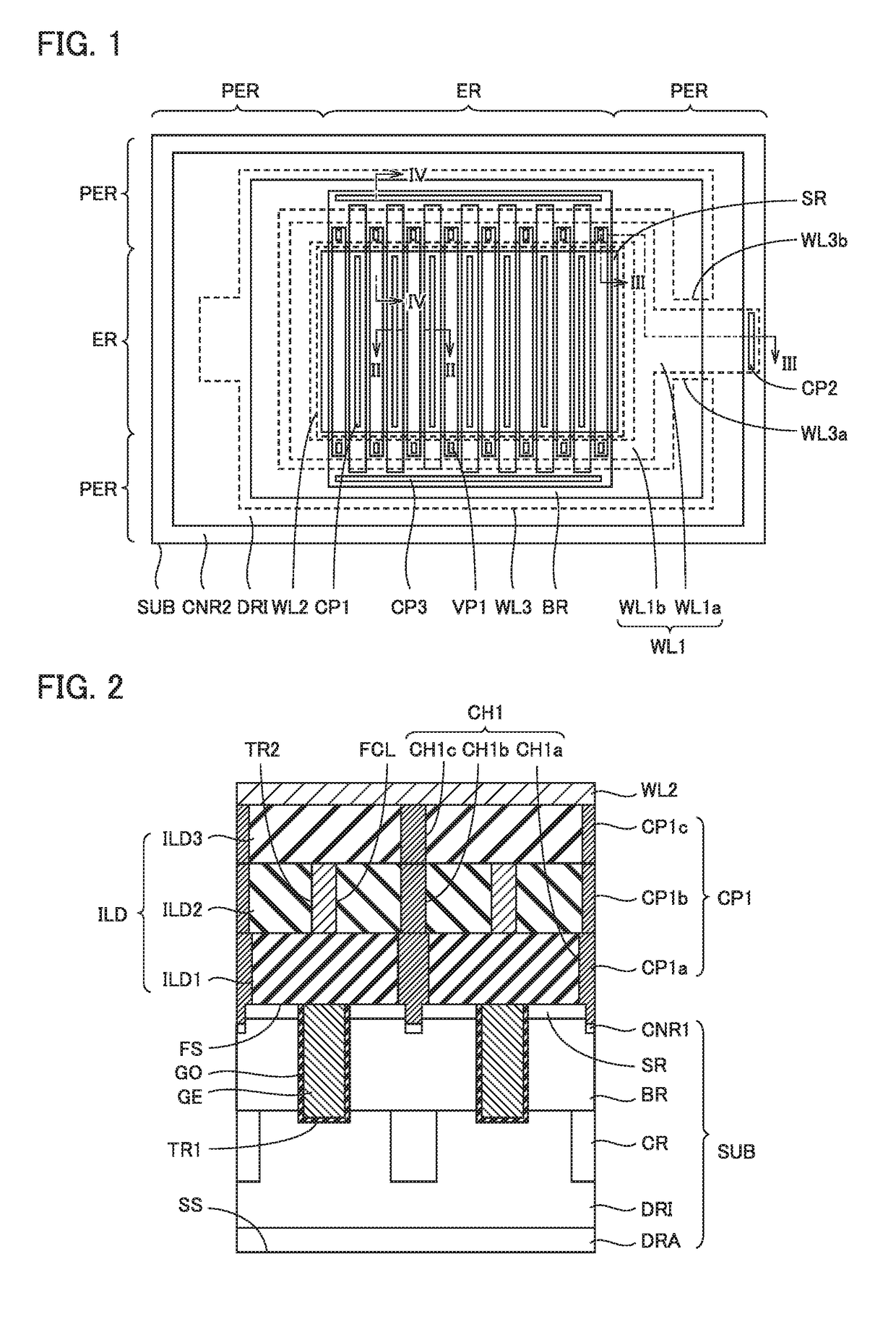
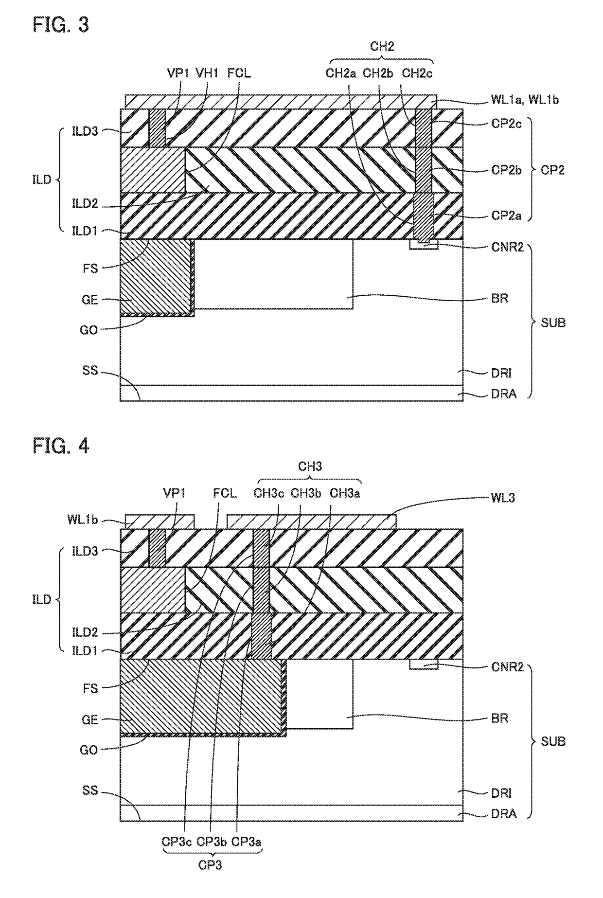
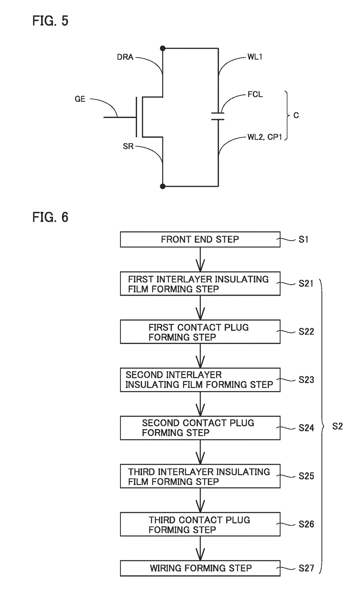
[0043]A structure of a semiconductor device according to a first embodiment will be described below.

[0044]As shown in FIGS. 1, 2, 3, and 4, the semiconductor device according to the first embodiment has a semiconductor substrate SUB, a gate insulating film GO, a gate electrode GE, an interlayer insulating film ILD, a contact plug CP1, a contact plug CP2, a contact plug CP3, a first conductive film FCL, a first wiring WL1, a second wiring WL2, and a third wiring WL3.

[0045]Semiconductor substrate SUB has an element region ER and an outer peripheral region PER. Outer peripheral region PER is located in an outer peripheral portion of semiconductor substrate SUB. Element region ER is a region inside a boundary between a source region SR and a body region BR in a plan view. Semiconductor substrate SUB has a first surface FS and a second surface SS. Second surface SS is an opposite surface of first surface FS. Semiconductor substrate SUB is made of, for example, monocrystalline silicon (Si...

second embodiment

[0098]A structure of a semiconductor device according to a second embodiment will be described below. In the following description, the differences from the structure of the semiconductor device according to the first embodiment will be mainly described and redundant description will not be repeated.

[0099]As shown in FIGS. 22, 23, 24, and 25, the semiconductor device according to the second embodiment has semiconductor substrate SUB, gate insulating film GO, gate electrode GE, interlayer insulating film ILD, contact plug CP1, contact plug CP2, contact plug CP3, first wiring WL1, second wiring WL2, third wiring WL3, via plug VP1, and first conductive film FCL. In regard to this point, the semiconductor device according to the second embodiment is in common with the semiconductor device according to the first embodiment.

[0100]The semiconductor device according to the second embodiment further has a second conductive film SCL, a via plug VP2 and a via plug VP3. In regard to this point,...

third embodiment

[0124]A structure of a semiconductor device according to a third embodiment will be described below. In the following description, the differences from the semiconductor device according to the second embodiment will be mainly described and redundant description will not be repeated.

[0125]As shown in FIGS. 26, 27, 28, and 29, the semiconductor device according to the third embodiment has semiconductor substrate SUB, gate insulating film GO, gate electrode GE, and interlayer insulating film ILD. The semiconductor device according to the third embodiment has contact plug CP1, contact plug CP2, contact plug CP3, first wiring WL1, second wiring WL2, third wiring WL3, via plug VP1, via plug VP2, via plug VP3, first conductive film FCL, and second conductive film SCL. In regard to these points, the semiconductor device according to the third embodiment is in common with the semiconductor device according to the second embodiment.

[0126]The semiconductor device according to the third embodi...


PUM


Abstract

A semiconductor device according to one embodiment includes: a semiconductor substrate having a first surface and a second surface which is an opposite surface of the first surface; a first wiring and a second wiring disposed on the first surface; a first conductive film electrically connected to the first wiring; and a gate electrode. The semiconductor substrate has a source region, a drain region, a drift region, and a body region. The drift region is disposed so as to surround the body region in a plan view. The first wiring has a first portion disposed so as to extend across a boundary between the drift region and the body region in a plan view, and electrically connected to the drift region. The second wiring is electrically connected to the source region. The first conductive film is insulated from and faces the second wiring.

Description

[0001]This nonprovisional application is based on Japanese Patent Application No. 2017-117572 filed on Jun. 15, 2017 with the Japan Patent Office, the entire contents of which are hereby incorporated by reference.BACKGROUND OF THE INVENTIONField of the Invention[0002]The present invention relates to a semiconductor device.Description of the Background Art[0003]Conventionally, a trench-gate-type and vertical MOSFET (Metal Oxide Semiconductor Field Effect Transistor) has, for example, been known as a power semiconductor device.[0004]When noise occurs in such a trench-gate-type and vertical MOSFET, the noise passes through a junction capacitance of a p-n junction formed between a drift region and a base region. However, when the noise has a low frequency, an impedance of the junction capacitance increases. This causes a problem of making it difficult for the noise to pass through the junction capacitance.[0005]As a semiconductor device for addressing this problem, a semiconductor devic...

Claims


Application Information

Patent Timeline
IPC IPC(8): H01L29/78H01L29/423H01L29/66
CPCH01L29/7813H01L29/42368H01L29/66734H01L21/76895H01L21/823475H01L23/5283H01L27/088H01L23/4824H01L29/7803H01L27/0251H01L23/60H01L24/30H01L23/49838
Inventor KUDOU, HIROYOSHITOKUDA, SATORUUCHIYA, SATOSHI
Owner RENESAS ELECTRONICS CORP
Why Eureka
Try Eureka