Voltage generating circuit

Inactive Publication Date: 2009-03-19
PANASONIC CORP
View PDF8 Cites 4 Cited by
  • Summary
  • Abstract
  • Description
  • Claims
  • Application Information

AI Technical Summary

Benefits of technology

[0015]Therefore, a main object of the present invention is to provide a voltage generating circuit configured to prevent the increase of current consumption and the increase of a chip area.

Problems solved by technology

The first problem is that the power reduction is unfavorably limited because the power supply voltage can only be reduced within a certain range.
In order to drive the voltage generating circuit thus constituted, it is necessary to supply the current obtained when the grayscale voltage is divided by several tens of k Ω. Further, when the buffers in the source drive are connected, input capacitance as much as the number of channels serves as a load in the case where all of the buffers are connected, which often results in the nF order resistance.
When such a load as relatively large resistance or capacitance is driven, it is difficult to drive it at a high speed by a voltage equal to or near the power supply voltage even though the rail-to-rail operational amplifier is used.
In the case where resistance is a load, the voltage is divided between the resistance as the load and the resistance in the γ generating circuit unless the output impedance is reduced, which causes an error in an output voltage to occur.
The third problem is that it is difficult even for the rail-to-rail operational amplifier to drive voltages in the voltage range including the power supply voltage and voltages near the power supply voltage because the output transistor is operated in a non-saturation region, which changes the output impedance, and as a result, an error in the output voltage occurs.

Method used


Image

  • Voltage generating circuit
  • Voltage generating circuit
  • Voltage generating circuit

Examples


embodiment 1

PREFERRED EMBODIMENT 1

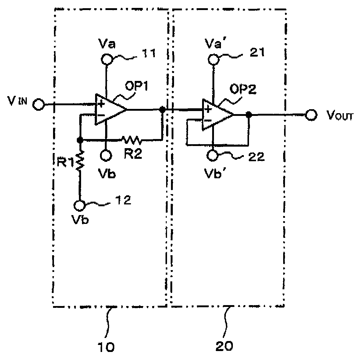
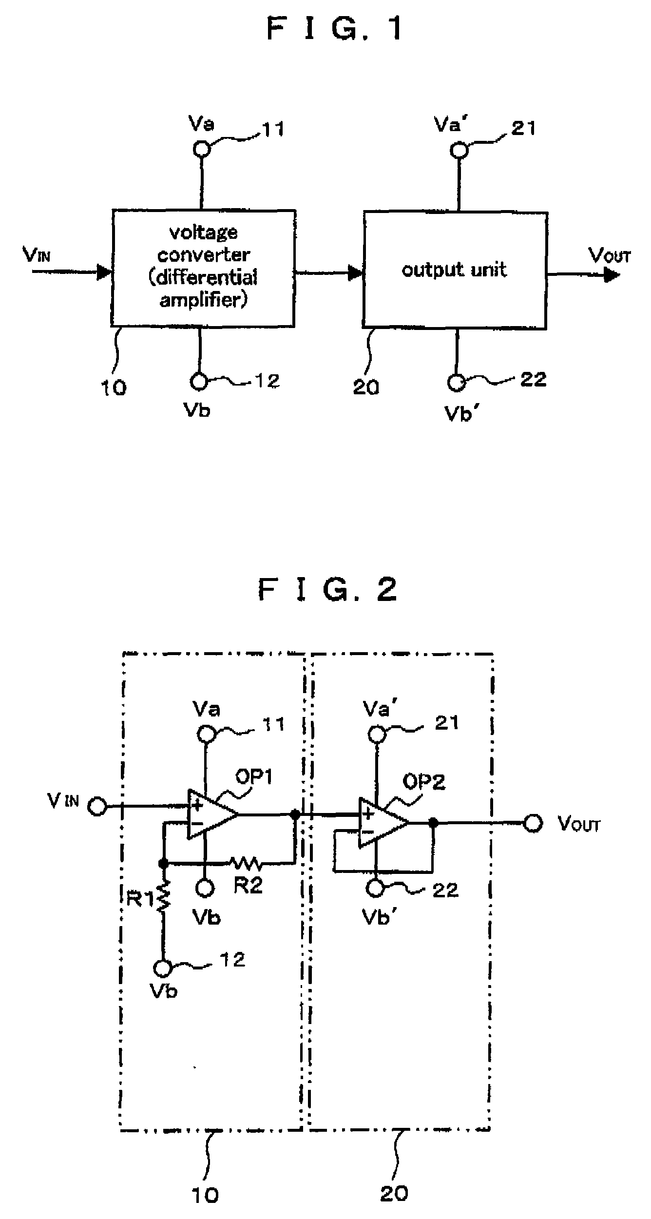
[0096]FIG. 1 is a block diagram illustrating a constitution of a voltage generating circuit according to a preferred embodiment 1 of the present invention. FIG. 2 is a circuit diagram more specifically illustrating the constitution shown in FIG. 1. The voltage generating circuit comprises a voltage converter (differential amplifier) 10 and an output unit 20. A non-inversion amplifier provided with an operational amplifier OP1, a resistance R1 and a resistance R2 constitutes the voltage converter (differential amplifier) 10. The operational amplifier OP1 comprises an input terminal, an inversion input terminal and an output terminal. A high-voltage-side power supply 11 (voltage Va) and a low-voltage-side power supply 12 (voltage Vb) are connected to the operational amplifier OP1. The output unit 20 comprises an operational amplifier OP2. The operational amplifier OP2 comprises an input terminal, an inversion input terminal and an output terminal, and constitutes...

modified embodiment 1

OF THE PREFERRED EMBODIMENT 1

[0118]In the case where the voltages near the power supply voltage Vb are generated contrary to the description so far, the power supply voltage Vb′ should be set to about −1.0V, and the power supply voltage Va′ should be set to 4.0V.

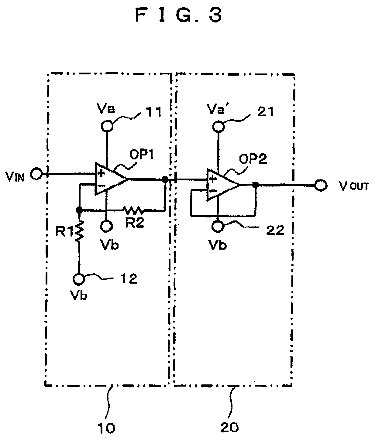
[0119]In the case where the output voltage range is narrow or a negative output voltage is generated, an inversion amplifier may be constituted by the operational amplifier OP1 and the resistances R1 and R2 constituting the voltage converter 10. In this constitution, the resistance R1 is connected to between the input terminal of the operational amplifier OP1 to which the input voltage VIN is inputted, and the inversion input terminal (−) of the operational amplifier OP1, and the resistance R2 is connected to between the inversion input terminal (−) and the output terminal of the operational amplifier OP1.

[0120]Furthermore, when the voltage Va is used as both of the voltage of the high-voltage-side power supply 11 in the vol...

modified embodiment 2

OF THE PREFERRED EMBODIMENT 1

[0121]Next, another modified embodiment, wherein LDO (Low Drop Out Regulator) is provided, is described. In FIG. 4, the same reference symbols as those shown in FIGS. 1, 2 and 3 denote the same components; therefore, those components will not be described in detail. A voltage generating circuit according to the present modified embodiment outputs a voltage while taking either of the following two ways: the way in which the current is discharged from the output; and the way in which the current is sucked into the output.

[0122]A reference symbol OP3 shown in the voltage converter 10 denotes a differential amplifying circuit. The high-voltage-side power supply 11 of the differential amplifying circuit OP3 is the power supply voltage Va, and the low-voltage-side power supply 12 thereof is the power supply voltage Vb. An output unit 20 comprises a drive transistor Q1 and resistances R3 and R4. Vc denotes a ground level. An output voltage VOUT is obtained by a...


PUM


Abstract

A voltage generating circuit according to the present invention comprises a voltage converter which voltage-converts a reference voltage, and an output unit which impedance-converts the voltage outputted from the voltage converter. The voltage converter and the output unit each comprise a low-voltage-side power supply and a high-voltage-side power supply. A voltage level of the high-voltage-side power supply in the output unit is set to be higher than a voltage level of the high-voltage-side power supply in the voltage converter.

Description

BACKGROUND OF THE INVENTION[0001]1. Field of the Invention[0002]The present invention relates to a voltage generating circuit comprising a voltage converter which inputs a reference voltage thereto and voltage-converting the inputted reference voltage, and an output unit which impedance-converts the voltage outputted from the voltage converter and outputs the converted voltage, more particularly to a technology for realizing such drive performance that achieve a high speed and a low impedance. The present invention is suitably applied, for example, to a liquid crystal display device wherein a liquid crystal display driver, a control circuit, RAM, and the like are mixedly provided.[0003]2. Description of the Related Art[0004]The following constitutions are conventionally known in an operational amplifier: a circuit configuration wherein a rail-to-rail operational amplifier is adopted to amplify an entire range of power supply voltages; and a configuration which realize a voltage gene...

Claims


Application Information

Patent Timeline
IPC IPC(8): G05F1/00
CPCG05F1/56H03F1/523H03F3/45475H03F3/505H03K17/0822H03F2203/45138H03F2203/45528H03F2203/5036H03F2203/5045H03F2200/444
Inventor KOJIMA, TOMOKAZU
Owner PANASONIC CORP
Why Eureka
Try Eureka