
Method and apparatus providing imager noise reduction using parallel input arithmetic mean modules

a technology of imager and arithmetic mean, applied in the field of semiconductor imager noise correction, can solve the problems of row noise still evident in the corrected image, fixed pattern noise generated from a mismatch of circuit structure, fixed pattern noise in the presence of cmos image sensor technology, etc., and achieve the effect of reducing noise in acquired images and facilitating calculation of averages and pixel offset values

Active Publication Date: 2007-01-25
APTINA IMAGING CORP
View PDF21 Cites 53 Cited by
  • Summary
  • Abstract
  • Description
  • Claims
  • Application Information

AI Technical Summary

Benefits of technology

[0009] The invention provides a method and apparatus that efficiently generates and applies noise correction values to the pixel outputs of a CMOS imager.
[0012] During image acquisition by the imager, noise in acquired images may be reduced by summing a digitized pixel output value with its corresponding offset value. Calculation of the averages and pixel offset values may be facilitated by the use of parallel input arithmetic mean modules.

Problems solved by technology

However, a drawback of the CMOS image sensor technology is the presence of fixed-pattern noise (FPN).
Fixed pattern noise is generated from a mismatch of circuit structures due to variations in the manufacturing processes of integrated circuits.
Even after correcting column-wise fixed pattern noise, row noise may still be evident in the corrected image.
In reality, however, significant differences in signal output values are read out between the pixel columns of the sensor array, even when a uniform input light stimulus is applied to the array.
The result is that the noise reduction processes add significant delay to the overall readout of the N by R pixel signals.

Method used


Image

  • Method and apparatus providing imager noise reduction using parallel input arithmetic mean modules
  • Method and apparatus providing imager noise reduction using parallel input arithmetic mean modules
  • Method and apparatus providing imager noise reduction using parallel input arithmetic mean modules

Examples


second embodiment

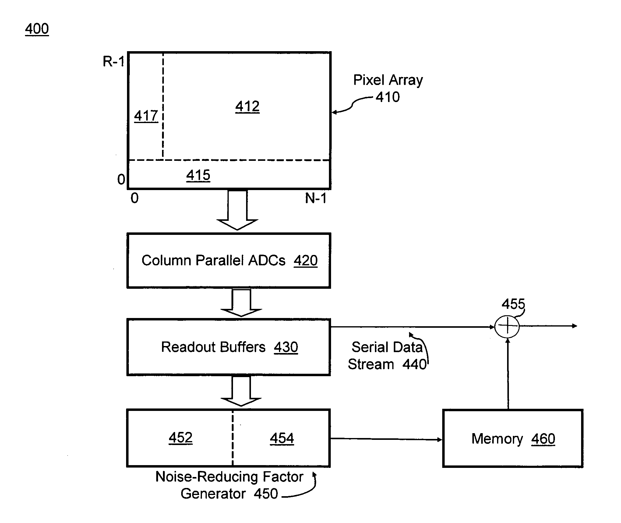
[0035] To ensure that pixels from different rows of the array are smoothed consistently, the row-noise correction module 454 (of FIG. 4) may be used in the invention. Referring again to FIG. 4, the row noise correction module 454 acts to generate noise-tolerant row-wise offset values. To accomplish this, the row noise correction module 454 reads pixel output signals originating from the row-wise calibration area 417. The pixels in the row-wise calibration area 417 are optically black pixels, meaning that the pixels in the row-wise calibration area 417 are not exposed to a light source. As a result, the pixel output signals from the pixels in the row-wise calibration area 417 represent signal-independent noise. As each row is read-out from the pixel array 410, pixel output signals from pixels within the row-wise calibration area 417 are input to the row noise correction module 454 in increments of n output signals. For each set of n output signals, an average output signal is calcula...

third embodiment

[0042]FIG. 9 is a flowchart summarizing the steps of the invention, as described above. Initially, a determination of whether calibration of the imager is necessary (see block 905). Calibration is necessary when the imager has first been turned on, when the operating mode of the imager has changed, or may be performed as desired. If it is determined that calibration is necessary, then a reference light or voltage signal is applied to the column-wise calibration area of the pixel array (block 910). All pixel outputs are then digitized, including the pixel outputs from the rows in the column-wise calibration area (block 915). In block 917, a decision is made as to which type of offset should be measured and applied. If column-wise offsets are to be determined, the column-wise calibration module reads n of the digitized pixel outputs from the column-wise calibration area (block 920). From those n pixel outputs, an average pixel output for the n pixel outputs is determined and the assoc...


PUM


Abstract

Noise correction values are generated through the calculation of pixel offset values and average pixel output values during a calibration procedure. For each read calibration row, an average pixel output value is determined for a plurality of pixel output values. An offset value for each of the plurality of pixel outputs is generated by finding the difference between each of the plurality of pixel outputs and the calculated average pixel output value. An offset value for an entire row of pixel outputs may also be calculated by finding the average pixel output value for a plurality of optically black pixels in the imager row. The average pixel output value for the optically black pixel values may be refined by discarding pixel values outside a threshold window and substituting the average pixel output value and calculate a new average pixel value.

Description

CROSS-REFERENCE TO RELATED APPLICATIONS [0001] This patent application claims priority to Japanese patent application No. 2005-211477 filed on Jul. 21, 2005 in the Japan Patent Office, the entire content of which is incorporated by reference herein.FIELD OF THE INVENTION [0002] The present invention relates generally to semiconductor imagers. More specifically, the present invention relates to noise correction in semiconductor imagers. BACKGROUND OF THE INVENTION [0003] Various types of imagers or image sensors are currently used, including charge-coupled device (CCD) image sensors and complementary metal-oxide semiconductor (CMOS) image sensors. CMOS technology offers many benefits, such as lower cost, ease of manufacturing, and a higher degree of integration over the CCD image sensors. However, a drawback of the CMOS image sensor technology is the presence of fixed-pattern noise (FPN). Fixed pattern noise is generated from a mismatch of circuit structures due to variations in the ...

Claims


Application Information

Patent Timeline
Patent Type & Authority Applications(United States)
IPC IPC(8): H04N5/217H04N25/00
CPCH04N25/677H04N25/76H04N25/618H04N25/78H04N25/633H04N25/671H04N25/63
Inventor SUZUKI, TOSHIKI
Owner APTINA IMAGING CORP
Learn More