Non-volatile memory device and methods of forming and operating the same

a memory device and non-volatile technology, applied in the direction of solid-state devices, semiconductor devices, instruments, etc., can solve the problems of inability to meet the requirements of the application, so as to improve the degree of cell integration and improve the distribution of threshold voltag

Active Publication Date: 2007-02-01
SAMSUNG ELECTRONICS CO LTD
View PDF7 Cites 4 Cited by
  • Summary
  • Abstract
  • Description
  • Claims
  • Application Information

AI Technical Summary

Benefits of technology

[0007] The present invention provides a non-volatile memory device capable of improving distribution of threshold voltage while improving the degree of cell integration.

Problems solved by technology

During the writing and erasing of a selected transistor, a disturbance can occur, where an unselected memory transistor sharing the common source line can inadvertently become written to or erased.
As a result, distribution of a threshold voltage becomes faulty.
However, since three transistors are required for this structure, the degree of device integration deteriorates.

Method used


Image

  • Non-volatile memory device and methods of forming and operating the same
  • Non-volatile memory device and methods of forming and operating the same
  • Non-volatile memory device and methods of forming and operating the same

Examples


Embodiment Construction

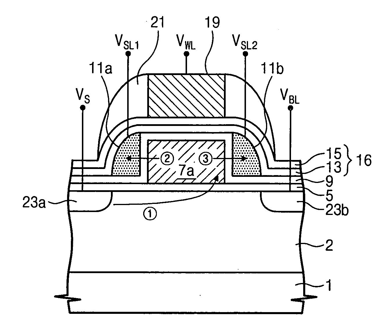
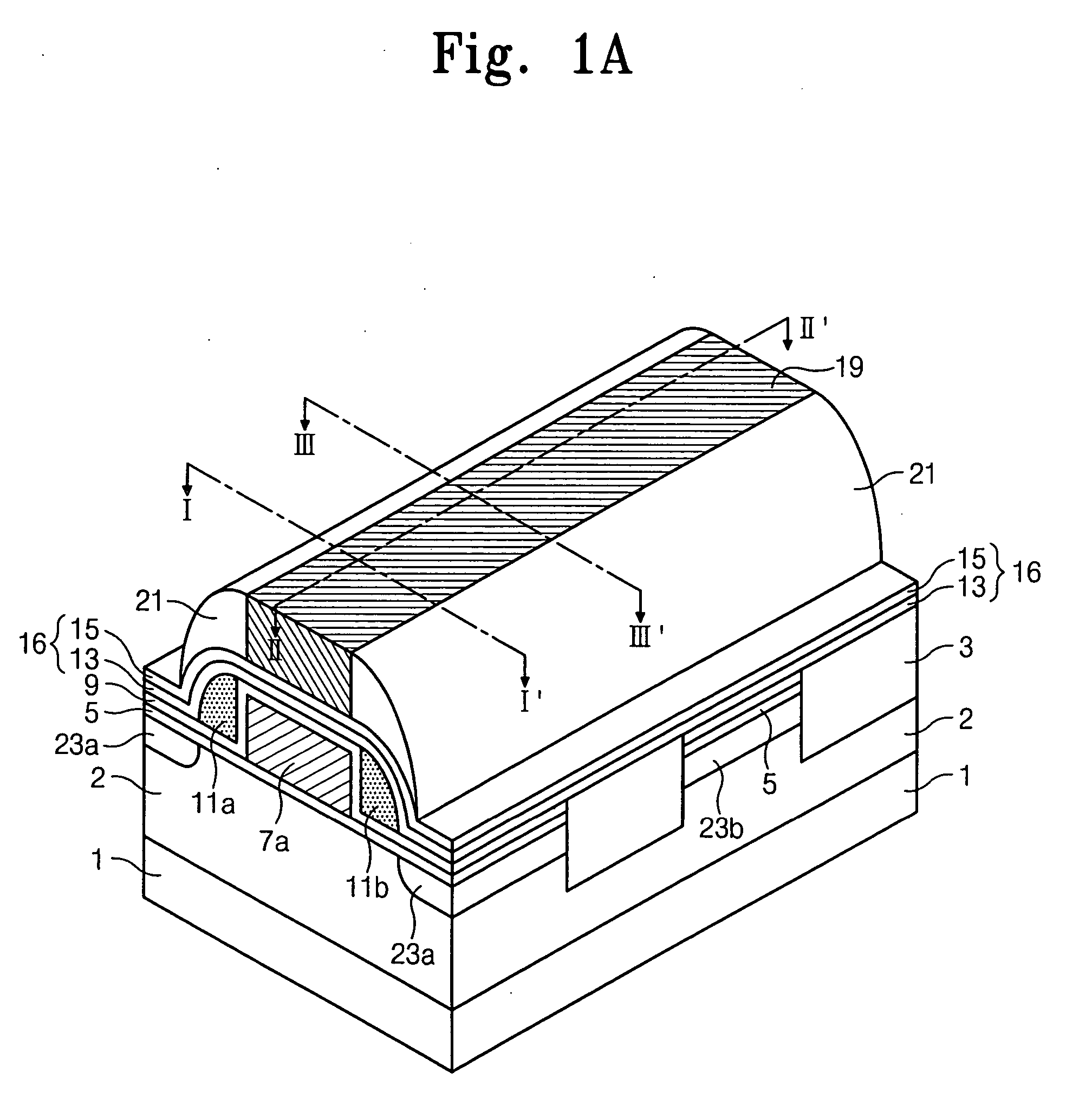
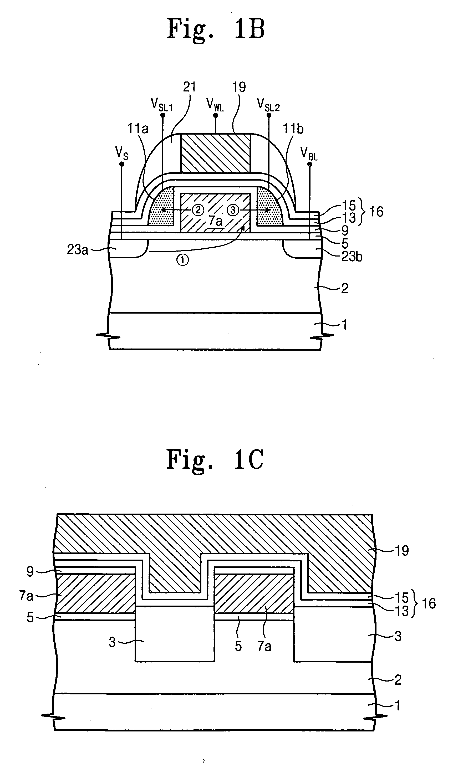
[0036] Reference will now be made in detail to the preferred embodiments of the present invention, examples of which are illustrated in the accompanying drawings. However, the present invention is not limited to the embodiments illustrated herein after, and the embodiments herein are rather introduced to provide ready and complete understanding of the scope and spirit of the present invention. In the drawings, the thickness of films and regions are exaggerated for clarity. In the drawings, the thickness of films and regions are exaggerated for clarity. It will also be understood that when a film is referred to as being on another film or substrate, it can be directly on the other film or substrate, or intervening films may also be present. Like reference numerals in the drawings denote like elements.

[0037]FIG. 1A is a perspective view of a non-volatile memory device according to an embodiment of the present invention. FIG. 1B is a sectional view taken along section line of I-I′ of ...


PUM


Abstract

In a non-volatile memory device and methods of forming and operating the same, one memory transistor includes sidewall selection gates covering both sidewalls of a floating gate when the floating gate and a control gate are stacked. The sidewall selection gates are in a spacer form. Since the sidewall selection gates are in a spacer form on the sidewall of the floating gate, the degree of integration of cells can be improved. Additionally, since the side wall selection gates are disposed on both sidewalls of the floating gate, a voltage applied from a bit line and a common source line can be controlled and thus conventional writing / erasing errors can be prevented. Therefore, distribution of threshold voltage can be improved.

Description

CROSS-REFERENCE TO RELATED PATENT APPLICATION [0001] This application claims priority to Korean Patent Application No. 10-2005-0069564, filed on Jul. 29, 2005, in the Korean Intellectual Property Office, the contents of which are incorporated herein by reference in their entirety. BACKGROUND OF THE INVENTION [0002] 1. Field of the Invention [0003] The present invention relates to a semiconductor device and methods of forming and operating the same, and more particularly, to a non-volatile memory device and methods of forming and operating the same. [0004] 2. Description of the Related Art [0005] In a non-volatile memory device, the structure of an Electrically Erasable Programmable Read-Only Memory (EEPROM) cell includes one memory transistor and one select transistor positioned between a common source line and a bit line. The memory transistor includes a floating gate that stores charge, a control gate formed on the top of the floating gate to control the floating gate, and a tunne...

Claims


Application Information

Patent Timeline
Patent Type & Authority Applications(United States)
IPC IPC(8): H01L29/788H01L21/8238
CPCG11C16/0425H01L27/115H01L29/7883H01L29/42328H01L27/11521H10B69/00H10B41/30
Inventor YANG, SEUNG-JINHAN, JEONG-UKKOH, KWANG-WOOKKIMPARK, SUNG-CHULKIM, JU-RI
Owner SAMSUNG ELECTRONICS CO LTD
Why Eureka
Try Eureka