Semiconductor devices having a recessed active edge and methods of fabricating the same

a technology of active edge and semiconductor, which is applied in the field of semiconductor devices having a recessed active edge, can solve the problems of reducing the driving current, increasing the contact resistance, and progressing the research into minimizing the 2-dimensional size of components such as transistors, and achieves high integration.

Active Publication Date: 2007-02-08
SAMSUNG ELECTRONICS CO LTD
View PDF6 Cites 18 Cited by
  • Summary
  • Abstract
  • Description
  • Claims
  • Application Information

AI Technical Summary

Problems solved by technology

Owing to the increased demand for highly integrated semiconductor devices, laborious research into minimizing the 2-dimensional sizes of components such as transistors has progressed.
However, the reduction in the channel length may cause some problems, such as the occurrence of punch-through, which leads to a reduction in the driving current.
The increase in the contact resistance deteriorates the current drivability of the MOS transistor.

Method used


Image

  • Semiconductor devices having a recessed active edge and methods of fabricating the same
  • Semiconductor devices having a recessed active edge and methods of fabricating the same
  • Semiconductor devices having a recessed active edge and methods of fabricating the same

Examples


Embodiment Construction

[0032] The present invention will now be described more fully hereinafter with reference to the accompanying drawings, in which exemplary embodiments of the invention are shown. This invention may, however, be embodied in different forms and should not be construed as limited to the embodiments set forth herein. Rather, these embodiments are provided so that this disclosure is thorough and complete and fully conveys the scope of the invention to those skilled in the art. In the drawings, the thicknesses of layers and regions are exaggerated for clarity and may not be to scale. It will also be understood that when a layer is referred to as being “on” another layer or substrate, it can be directly on the other layer or substrate or intervening layers may also be present. The same reference numerals are used to denote the same elements.

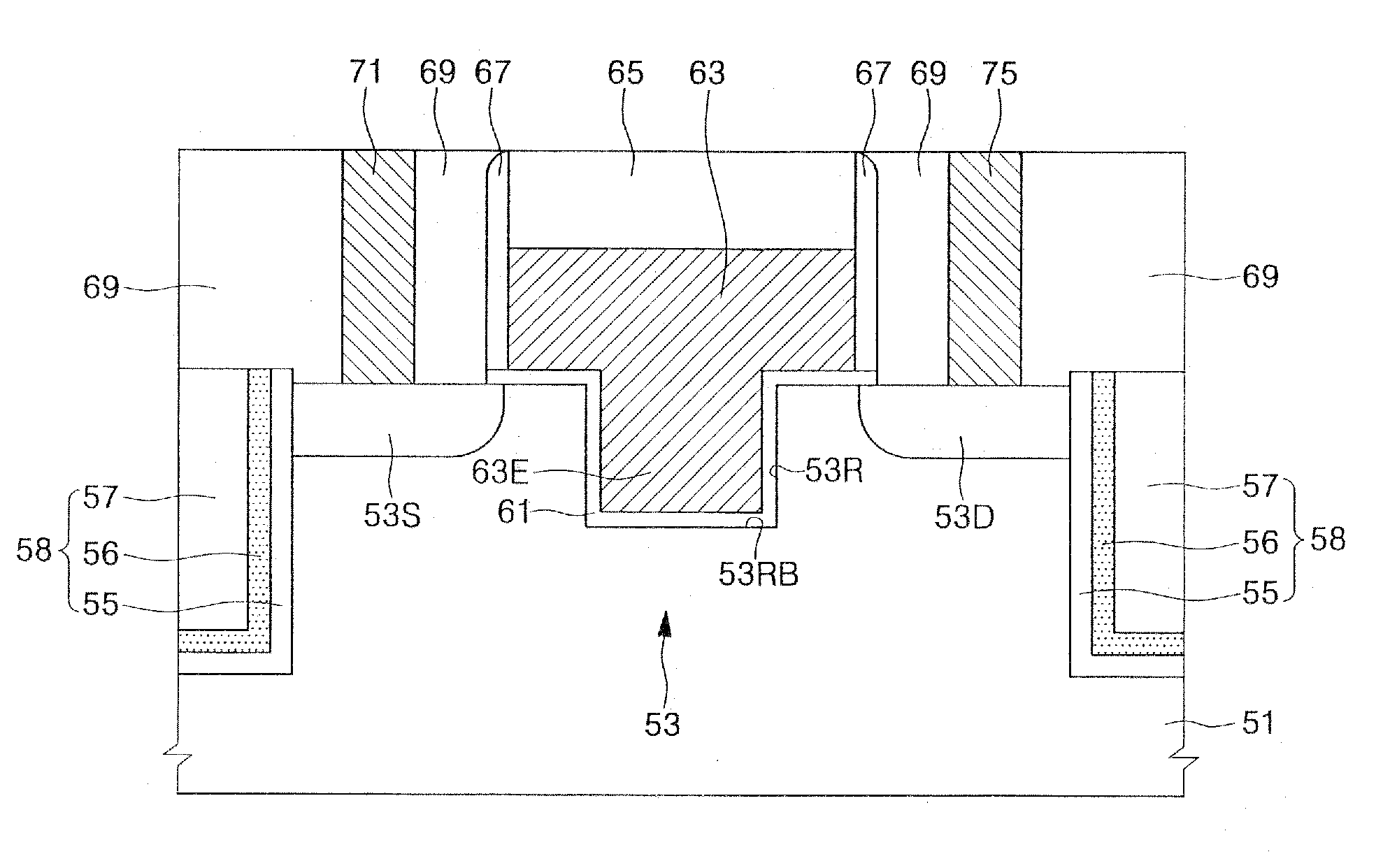
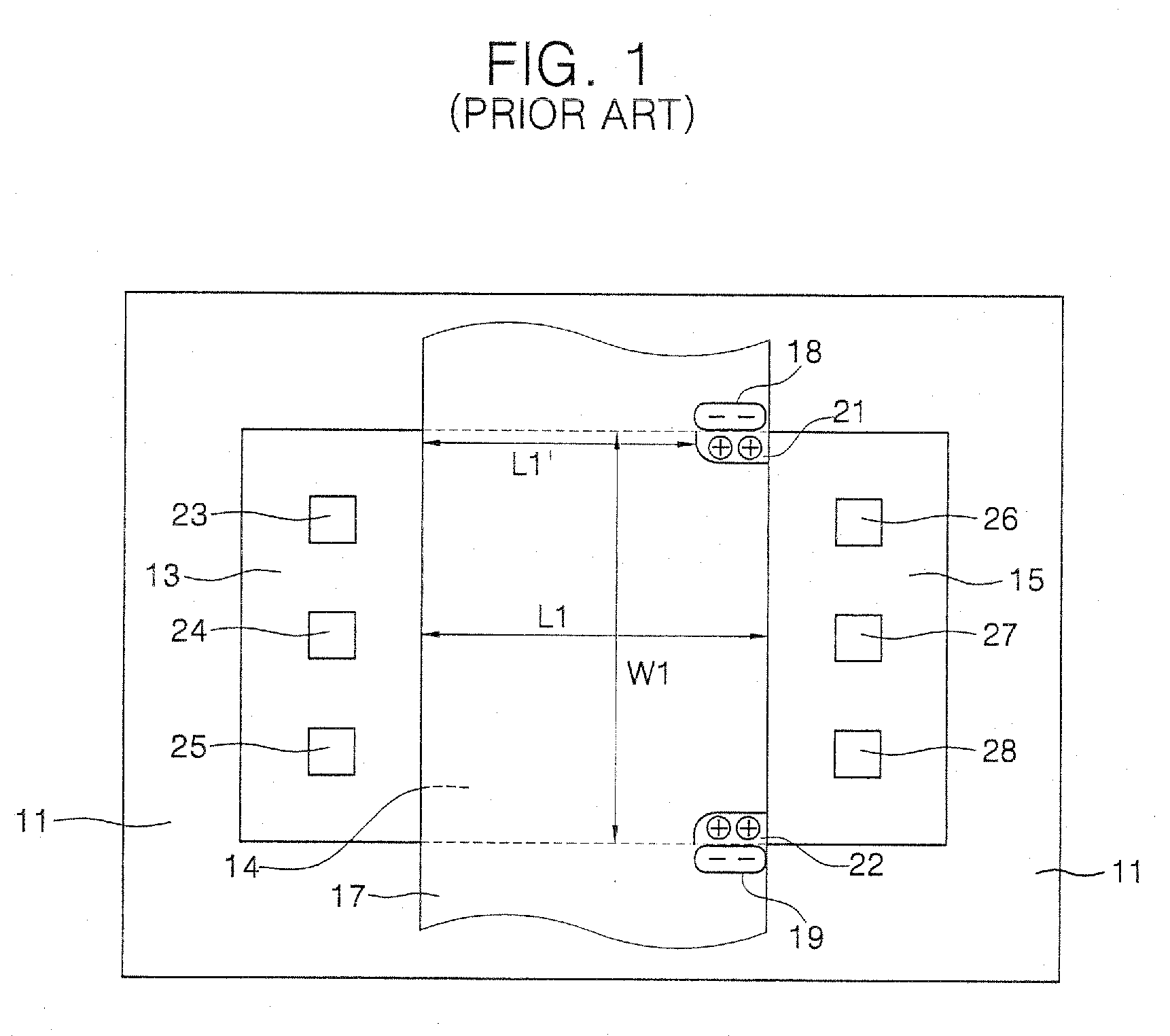
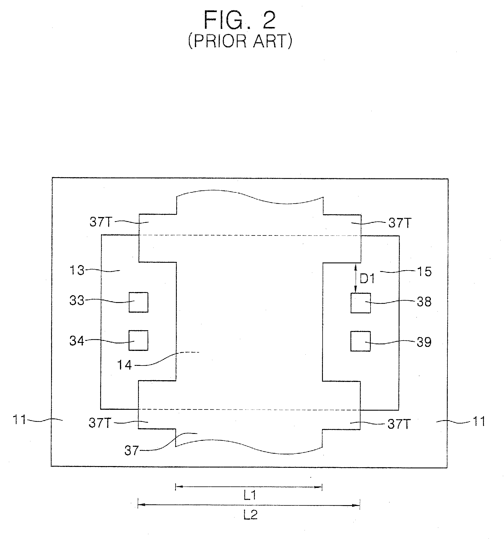
[0033]FIG. 3 shows the layout of a transistor having a recessed active edge according to an exemplary embodiment of the present invention, FIG. 4A is a...


PUM


Abstract

A semiconductor device having a recessed active edge is provided. The semiconductor devices include an isolation layer disposed in a substrate to define an active region. A gate electrode is disposed to cross over the active region. A source region and a drain region are disposed in the active region on both sides of the gate electrode. A recessed region is disposed under the gate electrode and on an edge of the active region adjacent to the isolation layer. A bottom of the recessed region may be sloped down toward the isolation layer. The gate electrode may further extend into and fill the recessed region. That is, a gate extension may be disposed in the recessed region. A method of fabricating the semiconductor device is also provided.

Description

[0001] This application claims the benefit of Korean Patent Application No. 2005-71915, filed Aug. 5, 2005, the contents of which are hereby incorporated by reference in their entirety. BACKGROUND [0002] 1. Field of the Invention [0003] The present invention relates to semiconductor devices and methods of fabricating the same, and more particularly, to semiconductor devices having a recessed active edge and methods of fabricating the same. [0004] 2. Description of Related Art [0005] Owing to the increased demand for highly integrated semiconductor devices, laborious research into minimizing the 2-dimensional sizes of components such as transistors has progressed. When a transistor is downscaled, the channel length and channel width also decrease. Because the driving current of the transistor is inversely proportional to the channel length and proportional to the channel width, a reduction in channel length can lead to a rise in driving current and an increase in the response speed. ...

Claims


Application Information

Patent Timeline
Patent Type & Authority Applications(United States)
IPC IPC(8): H01L29/94
CPCH01L21/28114H01L29/78H01L29/66621H01L29/42376H01L29/1037H01L29/4236
Inventor KIM, YONG-ILCHO, MIN-HEE
Owner SAMSUNG ELECTRONICS CO LTD
Why Eureka
Try Eureka