Method for regulating an output signal and circuit therefor

Active Publication Date: 2006-11-23
SEMICON COMPONENTS IND LLC
View PDF6 Cites 12 Cited by
  • Summary
  • Abstract
  • Description
  • Claims
  • Application Information

AI Technical Summary

Benefits of technology

[0005] The present invention satisfies the foregoing need by providing a circuit and a method for regulating an output signal. In accordance with one embodiment, the present invention includes a method for regulating an output signal

Problems solved by technology

However, it cannot be restarted until the next clock signal.
A drawback with this system is that if a transient electrical signal causes the output voltage to sag after the control signal has ended, the control signal will not compensat

Method used


Image

  • Method for regulating an output signal and circuit therefor
  • Method for regulating an output signal and circuit therefor
  • Method for regulating an output signal and circuit therefor

Examples


Embodiment Construction

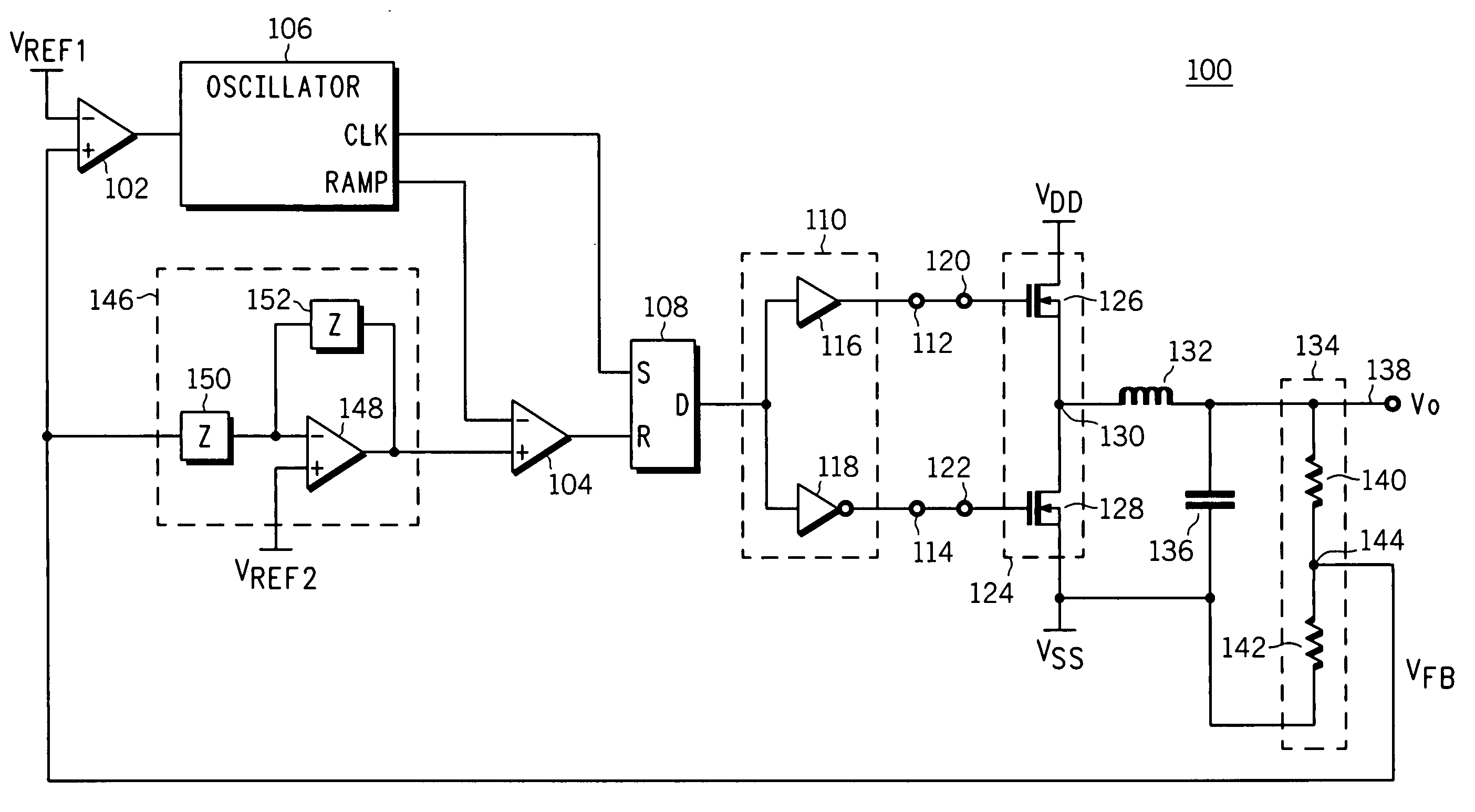
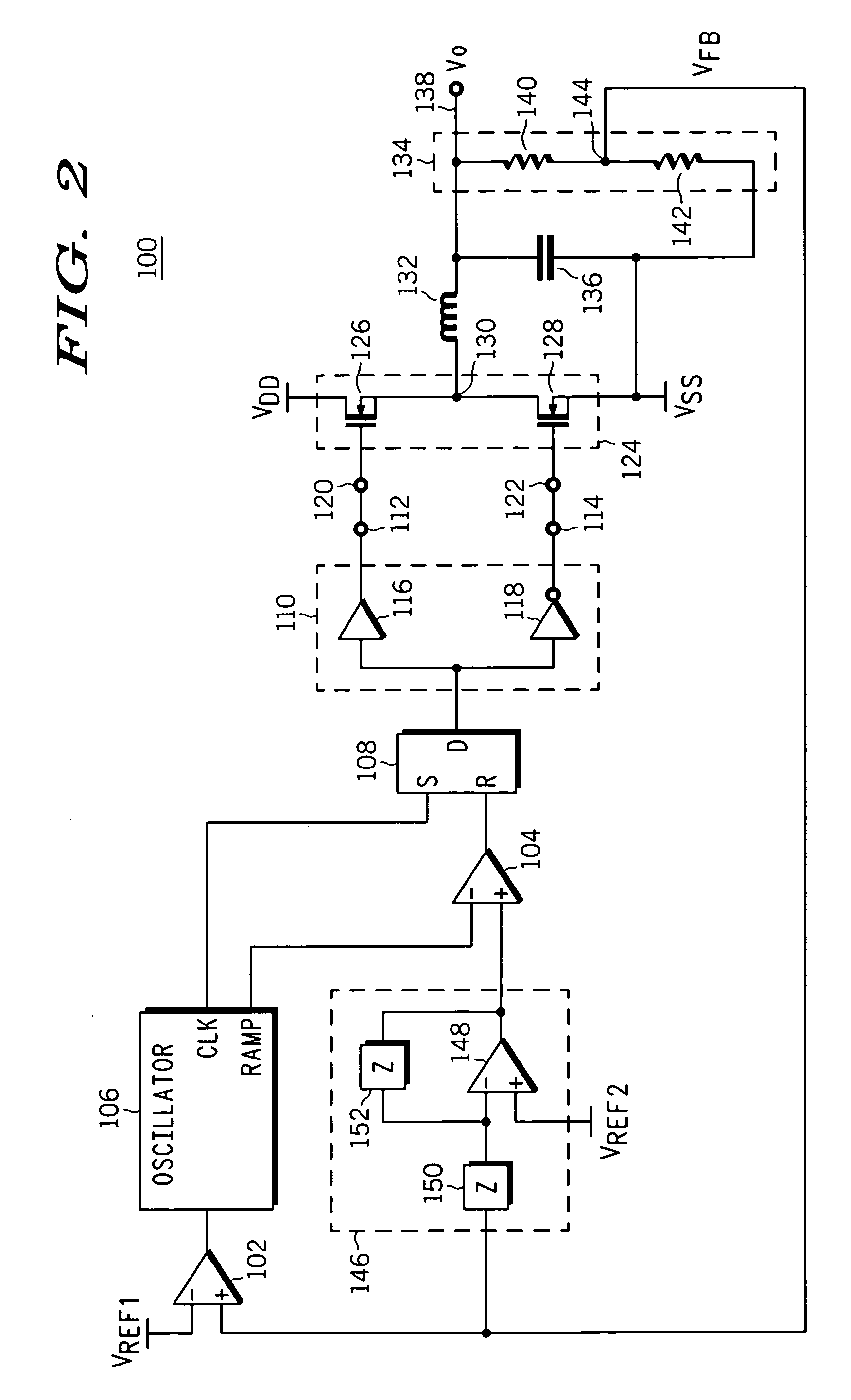
[0012]FIG. 2 is a schematic diagram of a switching power supply 100 in accordance with an embodiment of the present invention. Switching power supply 100 comprises differential comparators 102 and 104, an oscillator 106, a latch 108, a gate drive circuit 110, a switching network 124, a voltage divider network 134, and an error amplifier 146. More particularly, differential comparator 102 has a non-inverting input coupled for receiving a feedback voltage signal VFB from voltage divider network 134 and an inverting input coupled for receiving a reference voltage VREF1. The output of differential comparator 102 is coupled to an input of oscillator 106, which oscillator 106 has an output for transmitting a clock signal CLK and an output for transmitting a periodic signal RAMP. It should be noted that the periodic signal is designated RAMP because it is preferably a ramp signal. However, the periodic signal is not limited to being a ramp signal.

[0013] The output of oscillator 106 for tr...


PUM


Abstract

A regulator circuit and a method for compensating for sag in the output signal of the regulator circuit. A first comparator is coupled to an input of an oscillator, which oscillator outputs a clock signal and a ramp signal. In accordance with a feedback signal from the output of the regulator circuit, the clock and ramp signals of the oscillator are reset if the output signal sags to an undesirable level. The clock and ramp signals can be reset between active edges of the clock. The reset clock and ramp signals cause the regulator circuit to increase its output voltage to reduce the sag.

Description

FIELD OF THE INVENTION [0001] This invention relates, in general, to electronic circuits and, more particularly, to DC to DC converters. BACKGROUND OF THE INVENTION [0002] Switching power supplies are used in a variety of electronic products including computers, calculators, cell phones, cameras, Personal Digital Assistants (PDAs), video game controllers, etc. These types of supplies generate regulated voltages that are used to provide power for the integrated circuits contained in the electronic products. FIG. 1 illustrates a conventional switching power supply 10 that includes a switching regulator 12 having outputs coupled to the gates of switching transistors 14 and 16. A drain terminal of switching transistor 14 is coupled for receiving a source of operating potential VDD and a source terminal of switching transistor 14 is connected to a drain terminal of switching transistor 16. The common connection of the source and drain terminals of switching transistors 14 and 16 is conne...

Claims


Application Information

Patent Timeline
IPC IPC(8): G05F1/00
CPCY02B70/1466H02M3/1588Y02B70/10
Inventor STEELE, JEREMY F.
Owner SEMICON COMPONENTS IND LLC
Why Eureka
Try Eureka