Pixel circuit of organic electroluminescent display device and method of driving the same

Active Publication Date: 2007-02-22
SAMSUNG DISPLAY CO LTD
View PDF4 Cites 145 Cited by
  • Summary
  • Abstract
  • Description
  • Claims
  • Application Information

AI Technical Summary

Benefits of technology

[0023] An aspect of the present invention provides a pixel circuit of an organic electroluminescent display device and a method of driving the same in which a difference in threshold

Problems solved by technology

However, because the conventional pixel circuit needs three different scan lines Sn, AZn, and AZBn, the pixel circuit and the driving circuit are complicated and an aperture ratio of a light emitting display device including the pixel circuit is low.
Thus, a charging problem (or delay) makes it difficult to apply the con

Method used


Image

  • Pixel circuit of organic electroluminescent display device and method of driving the same
  • Pixel circuit of organic electroluminescent display device and method of driving the same
  • Pixel circuit of organic electroluminescent display device and method of driving the same

Examples


Example

FIRST EXEMPLARY EMBODIMENT

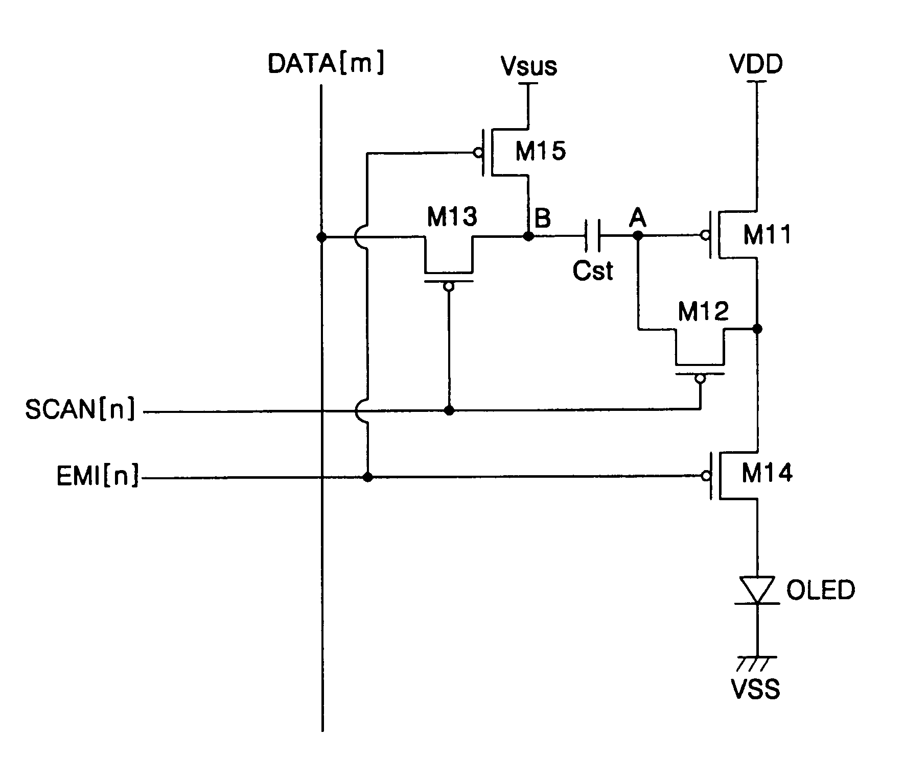
[0036]FIG. 3 is a circuit diagram of a pixel circuit of an organic electroluminescent display device according to a first exemplary embodiment of the present invention.

[0037] Referring to FIG. 3, the pixel circuit according to the first exemplary embodiment of the present invention includes first, second, third, fourth, and fifth transistors M11, M12, M13, M14 and M15, a capacitor Cst, and an organic EL diode OLED. In FIG. 3, the first, second, third, fourth, and fifth transistors M11, M12, M13, M14 and M15 are shown as P-channel metal oxide semiconductor field effect transistors (MOSFETs), but the present invention is not limited to any one kind of transistor (or carrier type); e.g., alternatively, the first, second, third, fourth, and fifth transistors may be N-channel MOSFETs.

[0038] The first (or driving) transistor M11 is connected between a power supply voltage VDD and the organic EL diode OLED and controls a driving current flowing in the organic E...

Example

[0061]FIG. 6 is a timing diagram for driving the pixel circuit according to the second exemplary embodiment of the present invention.

[0062] Referring to FIGS. 5 and 6, in an initialization period, when a low-level scan signal is applied from a scan line SCAN[n], a high-level previous emission control signal is applied from an emission control line EMI[n−1], and a low-level current emission control signal is applied from an emission control line EMI[n], the second (or threshold voltage compensation) transistor M12′, the third (or switching) transistor M13′, and the fourth (or emission control) transistor M14′ are turned on. Therefore, the voltage stored in the capacitor Cst′ in a previous frame is initialized through the threshold voltage compensation transistor M12′ and the emission control transistor M14′.

[0063] Unlike the first exemplary embodiment, in the pixel circuit according to the second exemplary embodiment of the present invention, the compensation voltage applying trans...


PUM


Abstract

A pixel circuit of an organic electroluminescent display device and a method of driving the same. In the pixel circuit, a capacitor has a first electrode connected to a gate of a driving transistor, and a second electrode connected to a drain of a switching transistor. Further, a compensation voltage applying transistor is connected to the second electrode of the capacitor. The compensation voltage applying transistor compensates for a difference in IR-drops of a power supply voltage in response to a previous emission control signal. Further, the compensation voltage applying transistor cuts off the compensation voltage in an initialization period, thereby preventing a source of a data voltage and a source of the compensation voltage from being shorted with each other. Additionally, a threshold voltage compensation transistor is connected between the gate and the drain of the driving transistor. Therefore, a difference in threshold voltages of driving transistors is compensated.

Description

CROSS-REFERENCE TO RELATED APPLICATION [0001] This application claims priority to and the benefit of Korean Patent Application No. 10-2005-0076994, filed Aug. 22, 2005 in the Korean Intellectual Property Office, the entire content of which is incorporated herein by reference. BACKGROUND OF THE INVENTION [0002] 1. Field of the Invention [0003] The present invention relates to an organic electroluminescent display device, and more particularly, to a pixel circuit of an organic electroluminescent display device and a method of driving the same. [0004] 2. Description of the Related Art [0005] An organic electroluminescent display device (or organic light emitting diode display device) is a flat panel display device that electrically excites an organic material (e.g., phosphorous organic compounds) to emit light. In an active matrix organic electroluminescent display device, a capacitor stores a voltage for representing a predetermined gray level, and the stored voltage is applied to a p...

Claims


Application Information

Patent Timeline
IPC IPC(8): G09G3/30
CPCG09G3/3233G09G2300/043G09G2300/0819G09G2300/0842G09G2300/0861G09G2310/0251G09G2310/0262G09G2320/043G09G3/30G09G3/20
Inventor KIM, YANG-WAN
Owner SAMSUNG DISPLAY CO LTD
Why Eureka
Try Eureka