
Semiconductor memory device having dummy sense amplifiers and methods of utilizing the same

a memory device and amplifier technology, applied in the direction of information storage, static storage, digital storage, etc., can solve the problems of increasing the size of the memory cell region and thus the chip size, unable to provide an unable to achieve easy layout of the sense amplifier, etc., to increase the sensing margin in sensing data, increase the redundancy efficiency, and increase the refresh margin

Inactive Publication Date: 2007-02-22
SAMSUNG ELECTRONICS CO LTD
View PDF5 Cites 28 Cited by
  • Summary
  • Abstract
  • Description
  • Claims
  • Application Information

AI Technical Summary

Benefits of technology

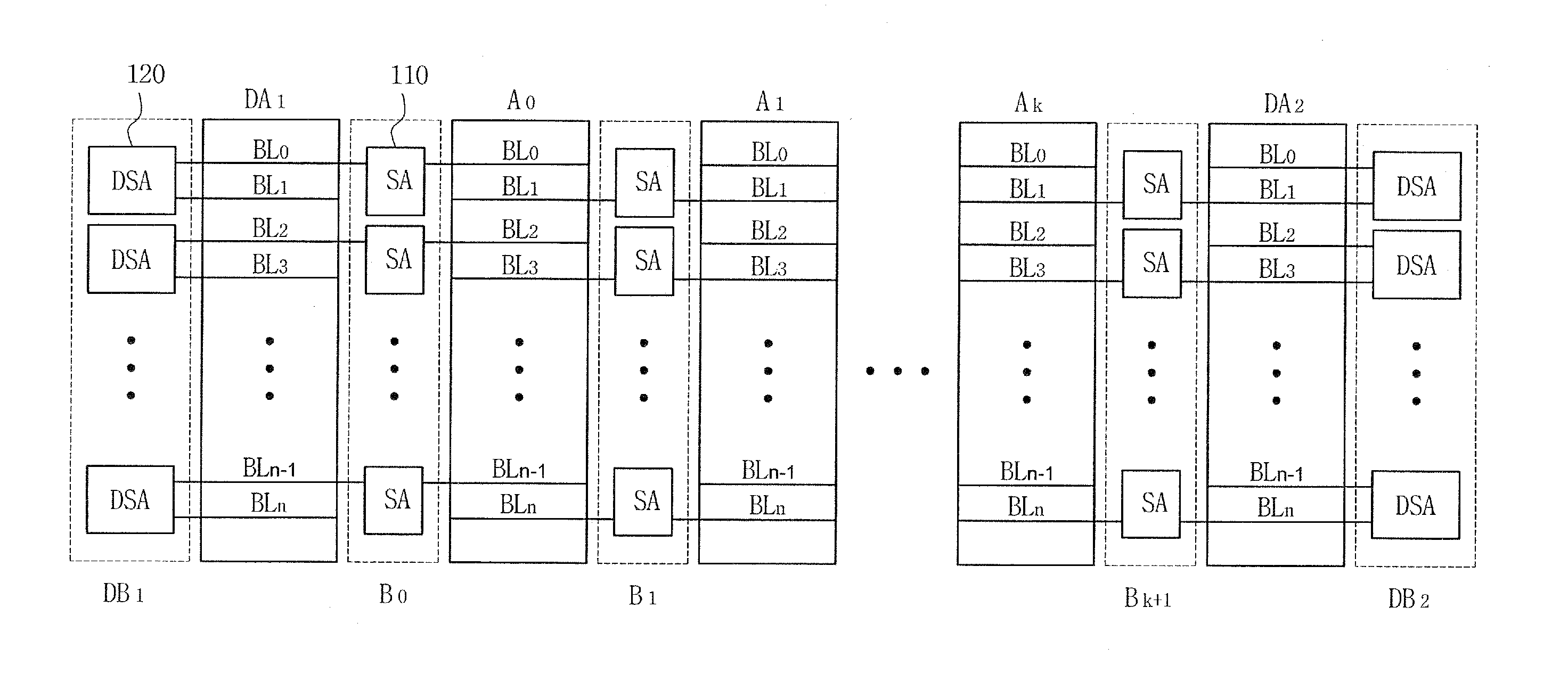
The present invention provides a semiconductor memory device with dummy sense amplifiers that can improve sensing margin, refresh margin, and redundancy efficiency by repairing normal cells. The device includes a dummy cell block with dummy cells and memory cells, and normal bit lines that connect the memory cells in a particular direction. Dummy bit lines connect the dummy cells together, and dummy sense amplifiers connect any two of the normal bit lines to the dummy bit lines. This helps to improve the efficiency and reliability of the memory device.

Problems solved by technology

However, since the sense amplifiers need to be laid out at every bit line pitch between two cell blocks, it is very difficult to lay out the sense amplifiers.
However, this may increase the size of the memory cell region and thus the chip size.
Among the sense amplifier implementing methods described above, the open bit line method requires a very strict design dimension of the sense amplifier and does not provide for an easy layout of the sense amplifier even though the memory cell area is small.
The folded bit line method can significantly reduce the design dimension of the sense amplifier, but increases the area of the memory cell and the chip size.

Method used


Image

  • Semiconductor memory device having dummy sense amplifiers and methods of utilizing the same
  • Semiconductor memory device having dummy sense amplifiers and methods of utilizing the same
  • Semiconductor memory device having dummy sense amplifiers and methods of utilizing the same

Examples


Embodiment Construction

[0024] The present invention will now be described more fully hereinafter with reference to the accompanying drawings, in which exemplary embodiments of the invention are shown. This invention may, however, be embodied in many different forms and should not be construed as being limited to the embodiments set forth herein. Rather, these embodiments are provided so that this disclosure will be thorough and complete, and will fully convey the scope of the invention to those skilled in the art.

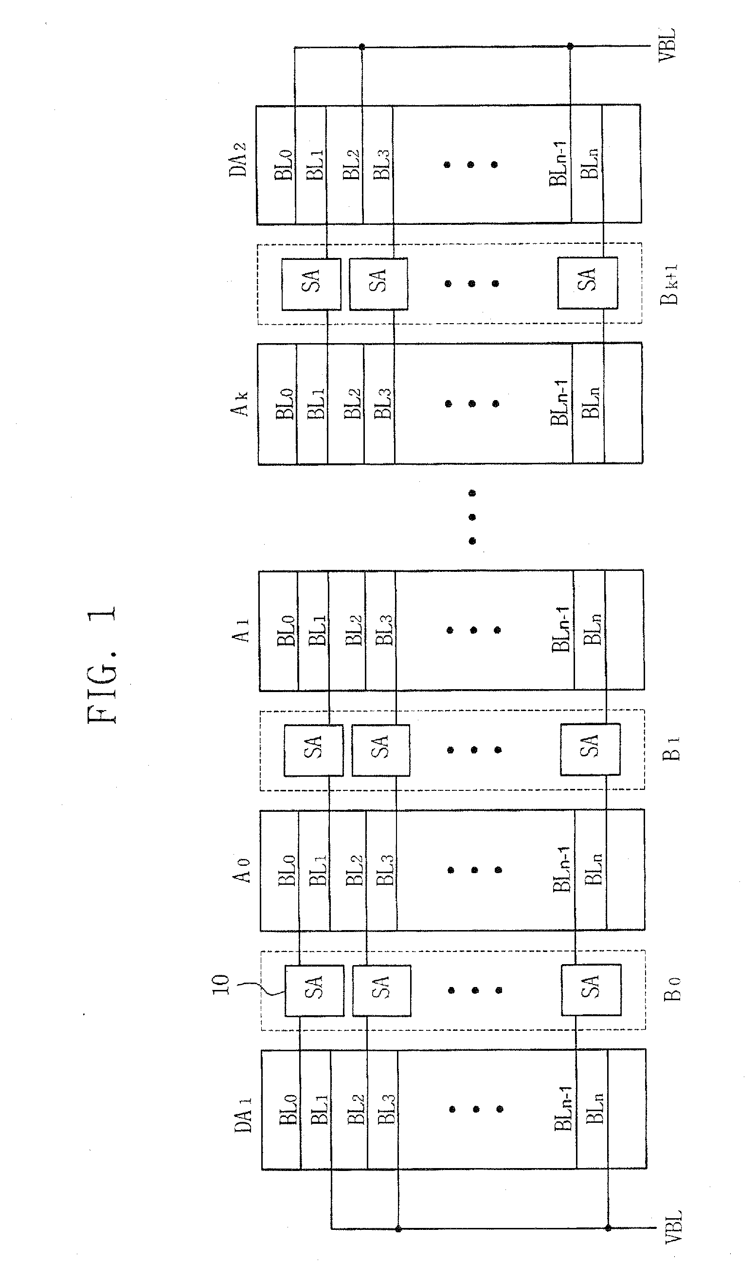
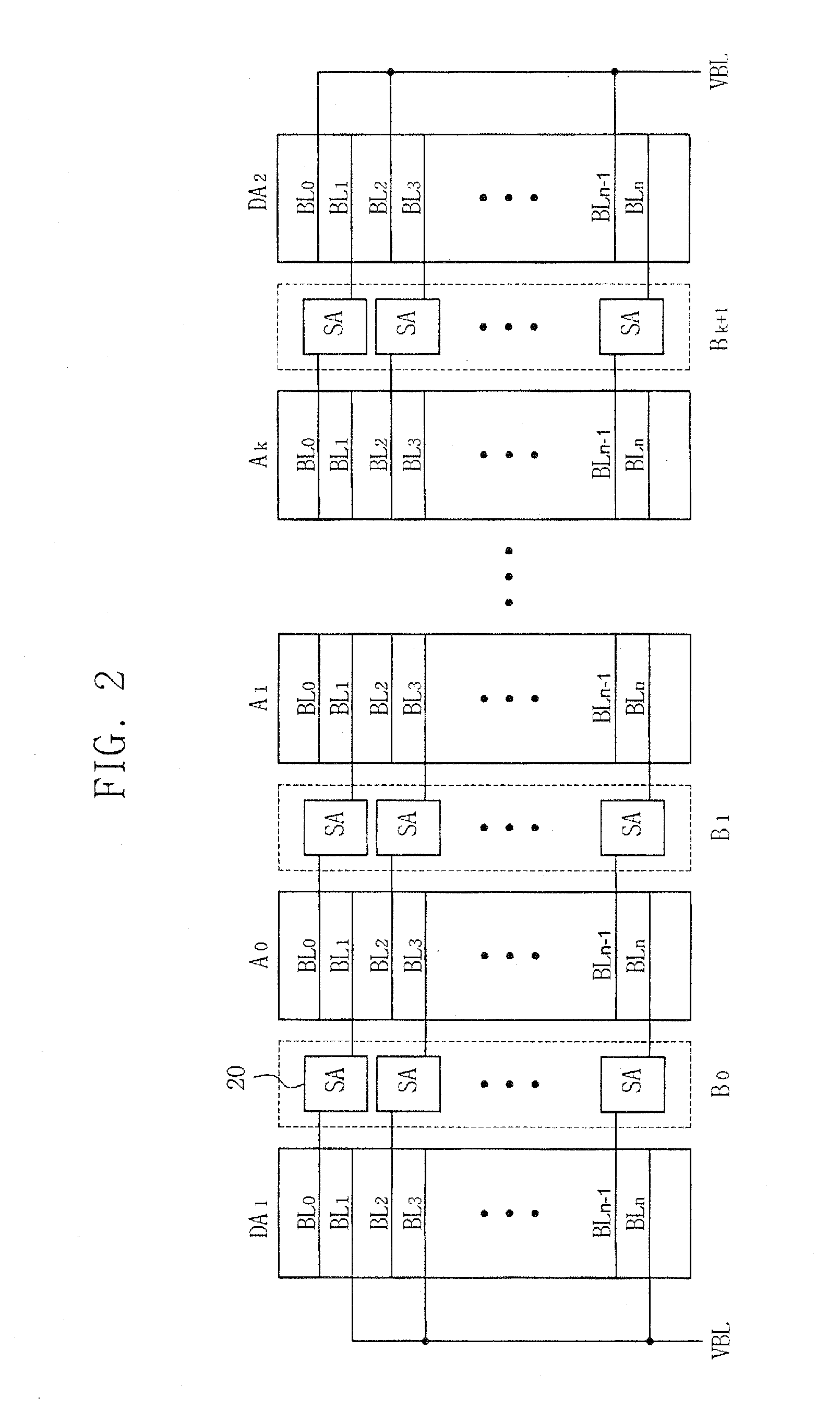
[0025]FIGS. 1 and 2 illustrate the structures of memory cell arrays using the relaxed open bit line method. The arrays of FIGS. 1 and 2 have the same structure except for the connection of sense amplifiers.

[0026] Referring to FIGS. 1 and 2, a memory cell array for a semiconductor memory device includes k+1 (k is a natural number) normal memory cell blocks A0 to Ak, and first and second dummy cell blocks DA1 and DA2.

[0027] The first dummy cell block DA1 is located at one edge of the normal memo...


PUM


Abstract

A semiconductor memory device having dummy sense amplifiers and a method of utilizing the same are provided. Embodiments of the semiconductor memory device may include at least one dummy cell block including dummy cells and memory cells. Normal bit lines connecting the memory cells in the dummy cell block in a first direction and dummy bit lines connecting the dummy cells in the first direction. A dummy sense amplifier is also included for connecting any two of the normal bit lines and the dummy bit lines. Some of the embodiments may improve the sensing margin and refresh margin in sensing memory cells in the dummy cell, as well as increasing the redundancy efficiency and utilization of the dummy cells.

Description

CROSS-REFERENCE TO RELATED APPLICATION [0001] This application claims the benefit of Korean Patent Application No. 10-2005-76281, filed Aug. 19, 2005, and Korean Patent Application No. 10-2006-12383, filed Feb. 9, 2006, the disclosures of which we incorporate by reference. BACKGROUND [0002] 1. Technical Field [0003] The present invention relates to a semiconductor memory device having dummy sense amplifiers and methods of utilizing the same, and more particularly, to a semiconductor memory device having dummy sense amplifiers and a methods of utilizing the same to maximize a refresh margin and a data sensing margin and to repair normal cells. [0004] 2. Discussion of Related Art [0005] In general, as semiconductor memory devices become more highly integrated and have increasingly high performance standards, the structure of a cell array including memory cells, bit lines, word lines, sense amplifiers, and the like in the semiconductor memory devices must be continually improved. [0006...

Claims


Application Information

Patent Timeline
Patent Type & Authority Applications(United States)
IPC IPC(8): G11C7/02
CPCG11C11/4091G11C11/4097
Inventor HONG, MIN-KIKANG, SANG-SEOKKIM, DONG-MIN
Owner SAMSUNG ELECTRONICS CO LTD
Learn More