Dual emission organic light emitting display device and method of driving the same

a display device and organic technology, applied in static indicating devices, thermoelectric devices, instruments, etc., can solve the problems of encapsulating such a device, high production cost, and application to a few number of applications

a display device and organic technology, applied in static indicating devices, thermoelectric devices, instruments, etc., can solve the problems of encapsulating such a device, high production cost, and application to a few number of applications

US20070045620A1Active Publication Date: 2007-03-01SAMSUNG DISPLAY CO LTD

Image

  • Dual emission organic light emitting display device and method of driving the same
  • Dual emission organic light emitting display device and method of driving the same
  • Dual emission organic light emitting display device and method of driving the same

Examples


embodiment 1

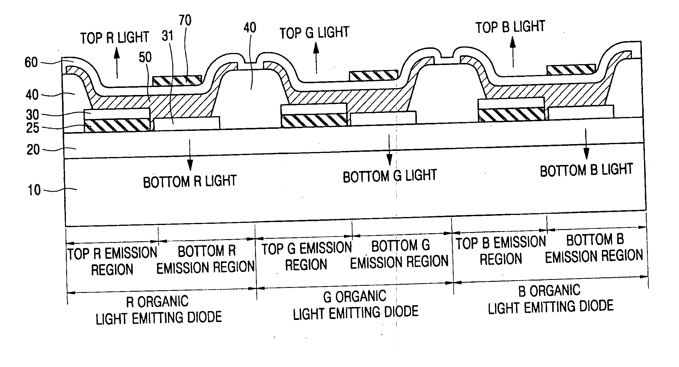
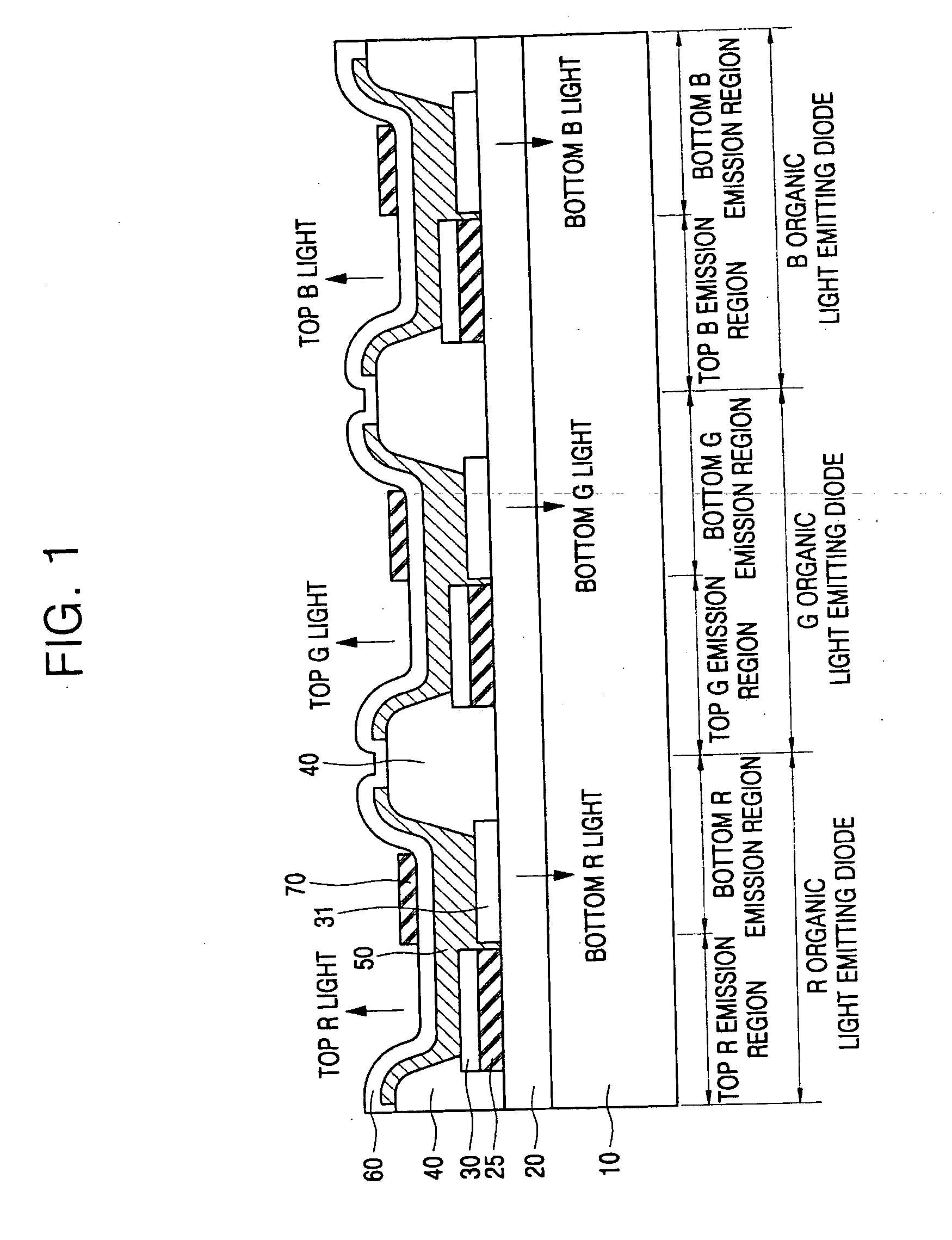
[0029]FIG. 1 is a cross-sectional view illustrating a process of fabricating red (R), green (G), and blue (B) organic light emitting diodes (OLEDs) of a dual emission organic light emitting display device according to an embodiment of the present invention.

[0030] Here, only a process of fabricating an R OLED will be described in detail for ease of explanation, and it should be understood by those skilled in the art that G and B OLEDs can be fabricated with substantially the same process.

[0031] Referring to FIG. 1, the R OLED is a dual emission R OLED and is divided into a top R emission region and a bottom R emission region.

[0032] The dual emission R OLED includes a glass substrate 10 on which thin film transistors (TFTs) (e.g., as show in FIG. 2) are formed to generate a driving current. The TFTs supply the driving current to the R OLED such that the dual emission R OLED emits light. The TFTs include a semiconductor layer formed by a low temperature polysilicon (LTPS) process. A...

embodiment 2

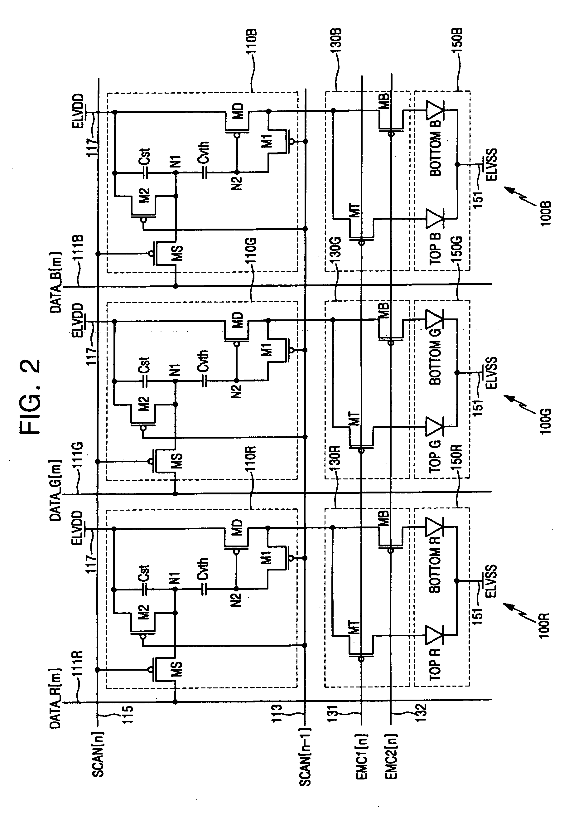
[0087]FIG. 4 is a circuit diagram of R, G, and B pixel circuits of a dual emission organic light emitting display device according to another embodiment of the present invention.

[0088] Referring to FIG. 4, one pixel circuit is divided into an R pixel circuit 200R, a G pixel circuit 200G, and a B pixel circuit 200B. Here, only the R pixel circuit 200R will be described in detail for ease of explanation.

[0089] The R pixel circuit 200R includes a pixel driver 210R, a top / bottom selector 230R, and an R OLED 250R.

[0090] The pixel driver 210R is enabled in response to a previous scan signal SCAN[n-1] and a current scan signal SCAN[n], receives an R data signal DATA_R[m] from a data line 211R, and generates a driving current. Also, the pixel driver 210R receives an emission control signal EMI[n] and allows or cuts off the flow of the driving current in response to the emission control signal EMI[n].

[0091] The top / bottom selector 230R allows the driving current to flow into a top R OLED...


PUM


Abstract

A dual emission organic light emitting display device and method of driving the same. The display device includes a pixel driver and an organic light emitting diode that can display different images on a top surface and a bottom surface and / or a same image on both the top and bottom surfaces. The display device includes a top / bottom selector that receives a driving current from the pixel driver and selectively supplies the driving current to a top organic light emitting diode or a bottom organic light emitting diode. The top / bottom selector includes transistors, which are connected between the pixel driver and the organic light emitting diode and select a top emission operation or a bottom emission operation. Here, the circuit configuration of the pixel driver is reduced so that the dual emission organic light emitting display device can be improved in terms of a layout, an interconnection, and an aperture ratio.

Description

CROSS-REFERENCE TO RELATED APPLICATION [0001] This application claims priority to and the benefit of Korean Patent Application No. 10-2005-0078758, filed Aug. 26, 2005, the entire content of which is incorporated herein by reference. BACKGROUND OF THE INVENTION [0002] 1. Field of the Invention [0003] The present invention relates to a dual emission organic light emitting display device, and more particularly, to a dual emission organic light emitting display device that can display different images on a top surface and a bottom surface and / or a same image on the top surface and the bottom surface using a single pixel driver, and a method of driving the same. [0004] 2. Description of the Related Art [0005] An organic light emitting display device is an emissive display in which light is created by electrically exciting organic compounds. That is, the organic light emitting display device includes an organic light emitting diode having an organic emission layer interposed between an a...

Claims


Application Information

Patent Timeline
01 Mar 2007
Publication
US20070045620A1
IPC
H01L29/08; H10N10/856
CPC
G09G3/3233; G09G2300/0804; G09G2300/0819; H01L27/3267; G09G2300/0861; G09G2320/043; G09G2300/0852; H10K59/128
Inventors
PARK, JIN-WOO; KWAK, WON-KYU