Output buffer circuit with de-emphasis function

a buffer circuit and function technology, applied in the field of semiconductor circuits, can solve the problems of reducing the efficiency of layout area and power efficiency, increasing the size of the main buffer, and reducing the efficiency of layout area and power, so as to reduce the number of circuit elements and reduce power consumption

Inactive Publication Date: 2007-03-01
RENESAS ELECTRONICS CORP
View PDF3 Cites 15 Cited by
  • Summary
  • Abstract
  • Description
  • Claims
  • Application Information

AI Technical Summary

Benefits of technology

[0038] In accordance with the present invention, the de-emphasis output buffer can be used as the main-data output buffer when the de-emphasis is disabled to optimize the entire circuit including a pre-buffer, to reduce the number of circuit elements, and to reduce power consumption.

Problems solved by technology

This makes the main buffer and large pre-buffer large and generates a problem that the efficiency of layout area and the power efficiency are greatly deteriorated.
The problem is that an increase in the main buffer size and the pre-buffer size greatly reduces the efficiency of the layout area and the power.

Method used


Image

  • Output buffer circuit with de-emphasis function
  • Output buffer circuit with de-emphasis function
  • Output buffer circuit with de-emphasis function

Examples


second embodiment

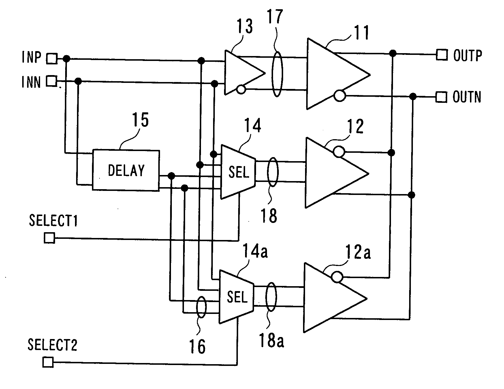
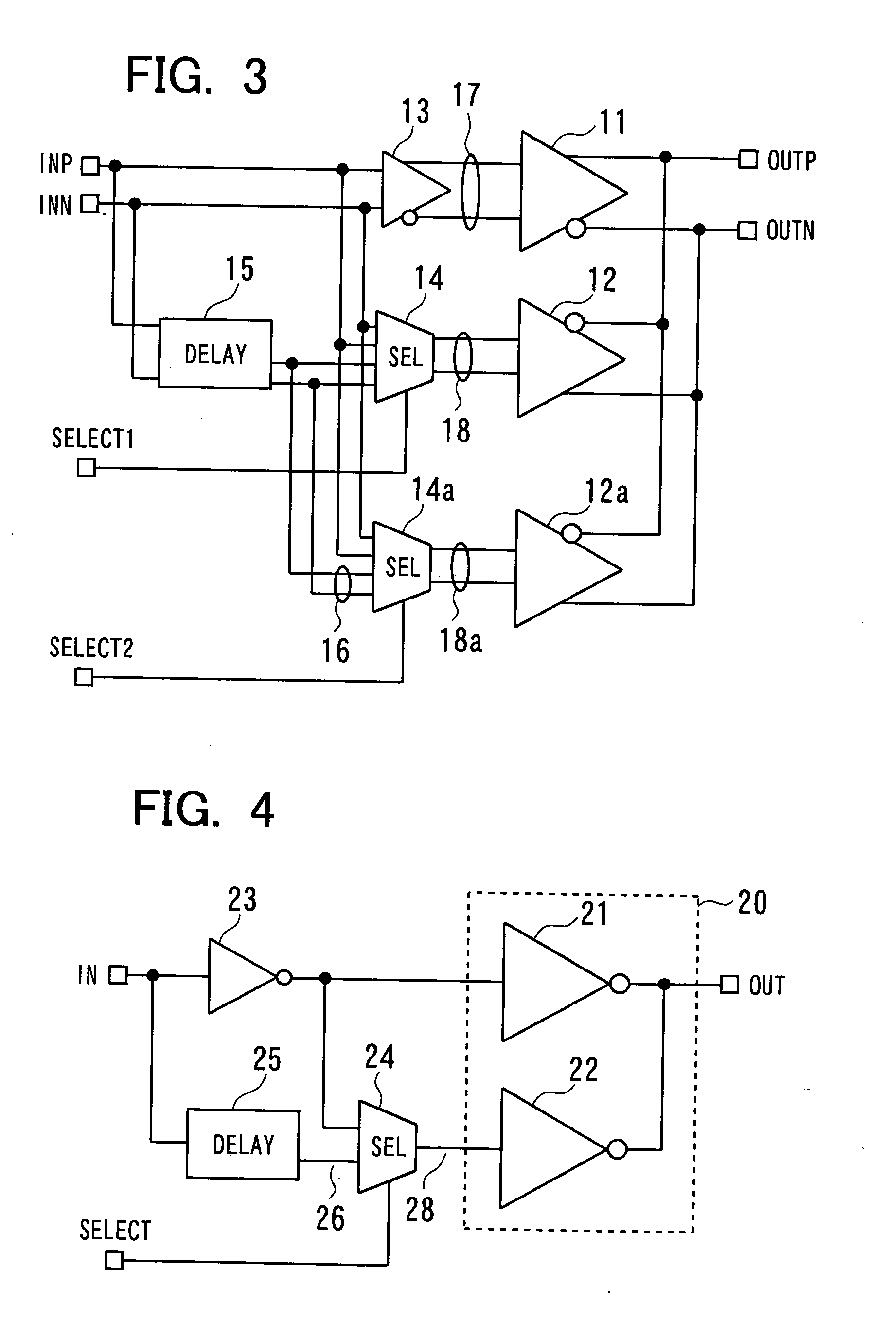
[0091] Next, another embodiment of the present invention will be described. FIG. 3 is a diagram showing the configuration of the present invention. This circuit is an output buffer circuit for which three types of de-emphasis level can be set. Like a selection circuit 14, a selection circuit 14a is a circuit that selects one of the following two signals based on a control signal SELECT2: a signal delayed by a delay circuit 15 and the inverting signal of original differential data signals 19.

[0092] Like a first de-emphasis main buffer 12, a second de-emphasis main buffer 12a is connected in such a way that subtraction is performed between a main-data main buffer 11 and the second de-emphasis main buffer 12a.

[0093] When the selection signals SELECT1 and SELECT2 have the logic value of 1 and the signals selected by the selection circuit 14 and selection circuit 14a are the output of the delay circuit 15, three types of emphasis amount can be set by the two-bit binary code. When the se...

third embodiment

[0100] The present invention is applicable also to an output buffer operating on a single-phase signal. FIG. 4 is a diagram showing the configuration of the present invention. Referring to FIG. 4, the output buffer circuit comprises an inverter 23 that inverts a data signal received by an input terminal IN; a main-data main buffer (inverter) 21 that receives the output of the inverter 23; a delay circuit 25 that delays the data signal received by the input terminal IN; a selector 24 that receives the output signal of the inverter 23 and the output of the delay circuit 25 and selects one of them based on the selection control signal SELECT; and a de-emphasis main buffer (inverter) 22 that receives the output of the selector 24.

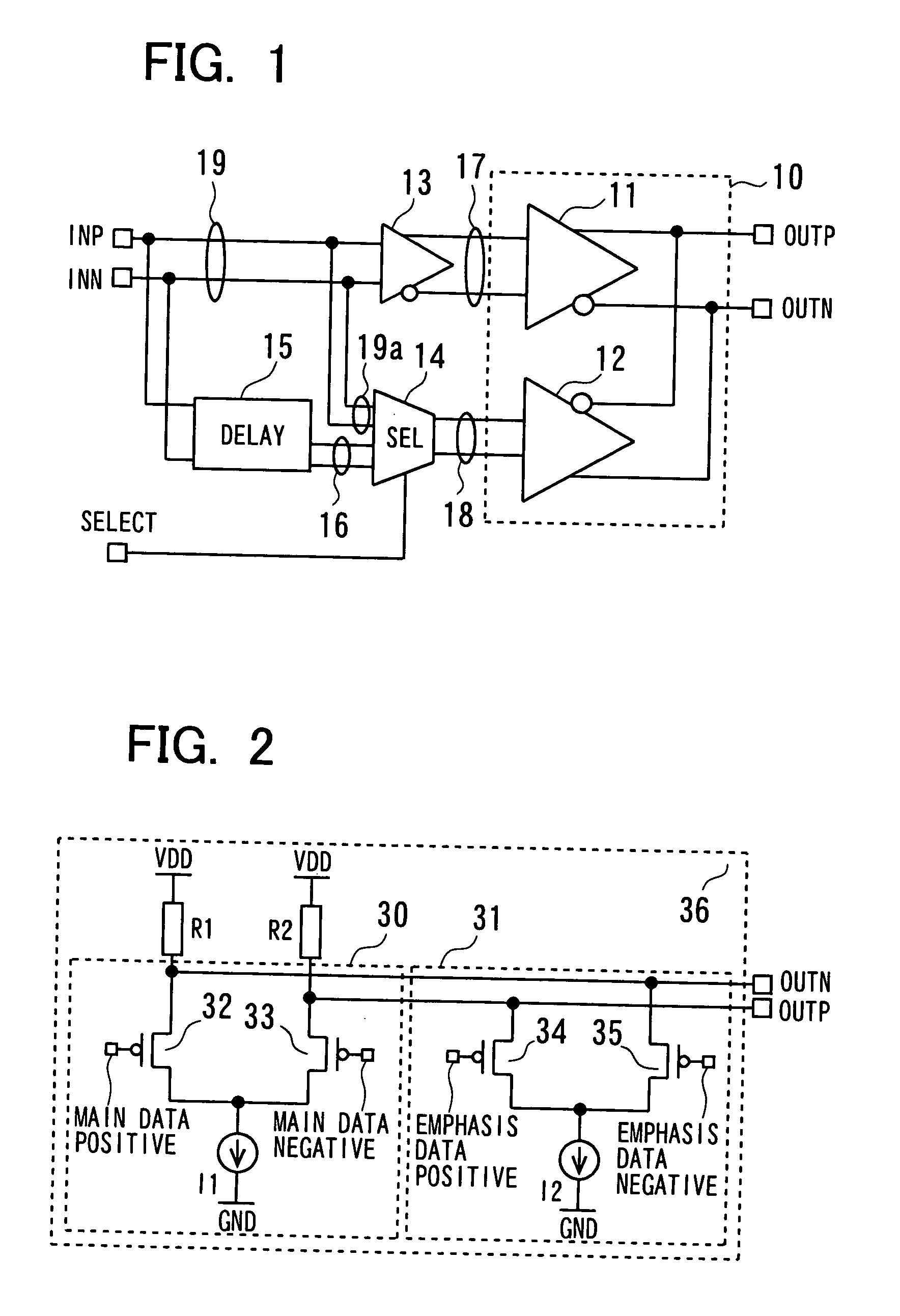
[0101]FIG. 5 is a diagram showing an example of a main buffer 20 comprising the main-data main buffer (inverter) 21 and the de-emphasis main buffer (inverter) 22 in FIG. 4. Referring to FIG. 5, the main buffer 21 corresponds to a main buffer 40, and the main bu...


PUM


Abstract

Disclosed is an output buffer circuit including main-data output buffers; a de-emphasis output buffer; and a selector that performs switching control in such a way that, based on a control signal indicating whether de-emphasis is to be enabled or disabled, main data is supplied to the de-emphasis output buffer to make the buffer operate as a main-data output buffer when the control signal indicates that de-emphasis is to be disabled, while emphasis data obtained on delaying the main data by the delay circuit is supplied to the de-emphasis output buffer to make the buffer operate as a de-emphasis output buffer when the control signal indicates that de-emphasis is to be enabled.

Description

FIELD OF THE INVENTION [0001] The present invention relates to a semiconductor circuit, and more particularly to an output buffer circuit with the de-emphasis function. BACKGROUND OF THE INVENTION [0002] Patent Documents 1 and 2 disclose an output buffer equipped with de-emphasis function in which the amplitude of an output signal emphasized when the logic of the output signal is changed, is attenuated when the logic of the output signal following the change remains unchanged. Patent document 1 discloses a configuration including a main buffer, a delay circuit, an emphasis driver, and a subtracter composed of a differential circuit. Patent Document 2 discloses an emphasis circuit constituted by a CMOS inverter, with a configuration including a tri-state buffer that performs switching control to determine whether to activate the emphasis function based on the control signal. [0003]FIG. 8 is a diagram showing the configuration of an output buffer circuit equipped with a conventional d...

Claims


Application Information

Patent Timeline
Patent Type & Authority Applications(United States)
IPC IPC(8): G06F13/00
CPCH04L25/0286H04L25/0272
Inventor TANAKA, MAKOTO
Owner RENESAS ELECTRONICS CORP
Why Eureka
Try Eureka