

Polishing pad, method of producing same and method of polishing
Inactive Publication Date: 2007-03-08
NIHON MICRO COATING
View PDF7 Cites 16 Cited by
- Summary
- Abstract
- Description
- Claims
- Application Information
AI Technical Summary
Benefits of technology
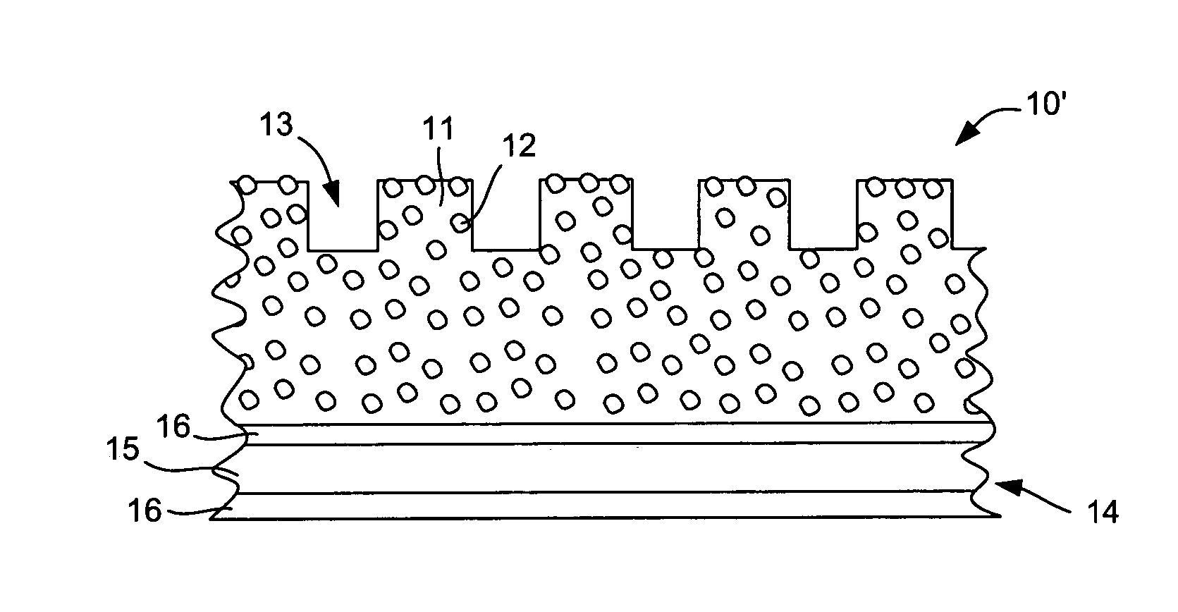
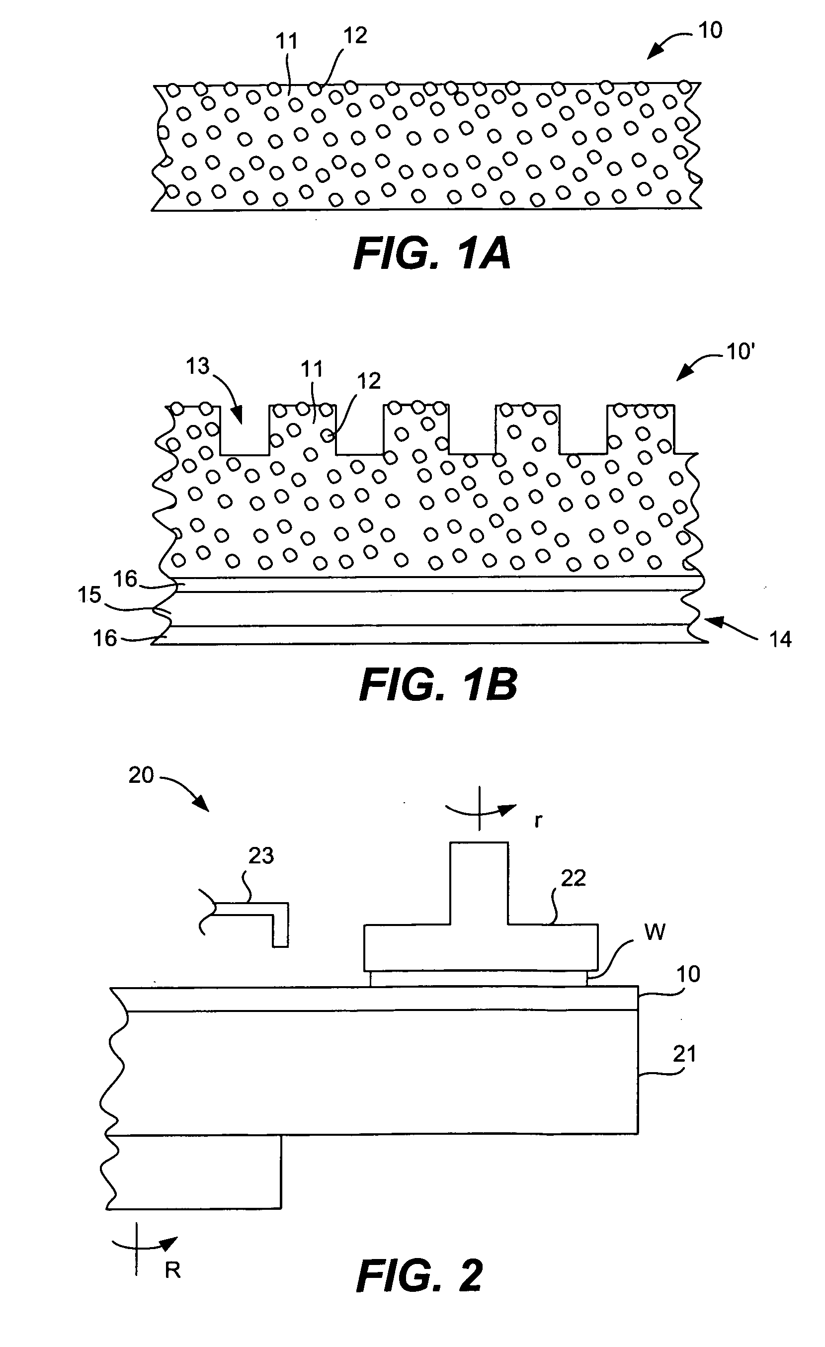
[0022] The merits of this invention are as follows. Firstly, since the tensile strength of the polishing pad is within the specified range described above, the surface of the workpiece can be pressed uniformly. Secondly, since the tensile tear elongation of the polishing pad is within the specified range described above, the force for fixing the abrading particles in the resin sheet is lowered such that the abrading particles drop off easily during the polishing process and since both the particles that have fall
Problems solved by technology
In a multi-layer wiring process or a film deposition process, such as mentioned above, however, if a next layer is formed over an underlying layer with an uneven surface, the upper surface of the subsequently formed upper layer (such as the surface of a multi-layer structure of a semiconductor device wafer) becomes uneven similarly to the uneven surface of the underlying layer therebelow.
If this surface of the upper layer thus formed is polished by using a polishing pad which is soft and flexible as described above, a gentle unevenness is formed on the surface, caused by this uneven upper surface, and the surface of the workpiece cannot be flattened to a desired high level of accuracy.
Since larger abrading particles tend to form unwanted scratched on the surface, however, it becomes difficult to obtain a flattened surface without scratches.
If abrading particles of a smal
Method used
View moreImage
Smart ImageViewing Examples

Examples
 PUM
| Property | Measurement | Unit |
|---|---|---|
| Diameter | aaaaa | aaaaa |
| Diameter | aaaaa | aaaaa |
| Diameter | aaaaa | aaaaa |
Abstract
A polishing pad has a resin sheet having a flat surface and abrading particles fixed inside and on the surface of this resin sheet. Its tensile strength is in the range of 30MPa or greater and 70 MPa or less and preferably in the range of 40MPa or greater and 60MPa or less. Its tensile tear elongation is in the range of 50% or less, preferably 20% or less and more preferably 5% or less. The average diameter of the primary particles of the abrading particles is in the range of 0.005 μm or greater and less than 0.5 μm, and preferably in the range of 0.005 μm or greater and 0.2 μm or less. The content of the abrading particles fixed to the resin sheet is 10 volume % or greater and 50 volume % or less, or preferably 10 volume % or greater and 24 volume or less.
Description
[0001] Priority is claimed on Japanese Patent Application 2005-260273 filed Sep. 8, 2005. BACKGROUND OF THE INVENTION [0002] This invention relates to a polishing pad used for polishing the surface of a workpiece made of a material such as metals, glass and crystals and more particularly a workpiece with a surface requiring a high level of flatness such as a semiconductor wafer, a semiconductor device wafer, a liquid crystal display element, a thin-film audio-visual device, a magnetic disk substrate, an optical disk substrate and a crystal substrate such as a quartz substrate, as well as a method of its production and a method of polishing. [0003] Semiconductor devices and magnetic disks are used as main components of electronic apparatus such as telephones, cameras and computers for controlling functions and storing and displaying data. The surface of a workpiece such as a semiconductor device wafer used in such an electronic component undergoes various processes required for the p...
Claims
Login to View More Application Information
Patent Timeline
 IPC IPC(8): B24B1/00B24B7/30B24D11/00
CPCB24D3/28B24B37/245
InventorWATANABE, JUNNAGAMINE, TAKUYATAMURA, JUNARAHATA, TAKASHI
OwnerNIHON MICRO COATING