

Burn-in system
a technology of burning system and burner, which is applied in the direction of electrical testing, measuring devices, instruments, etc., can solve the problems of difficult to apply uniform thermal stress to the simultaneously tested plurality of electronic devices, and the differences of each electronic devi
- Summary
- Abstract
- Description
- Claims
- Application Information
AI Technical Summary
Benefits of technology
Problems solved by technology
Method used
Image

Examples
first embodiment
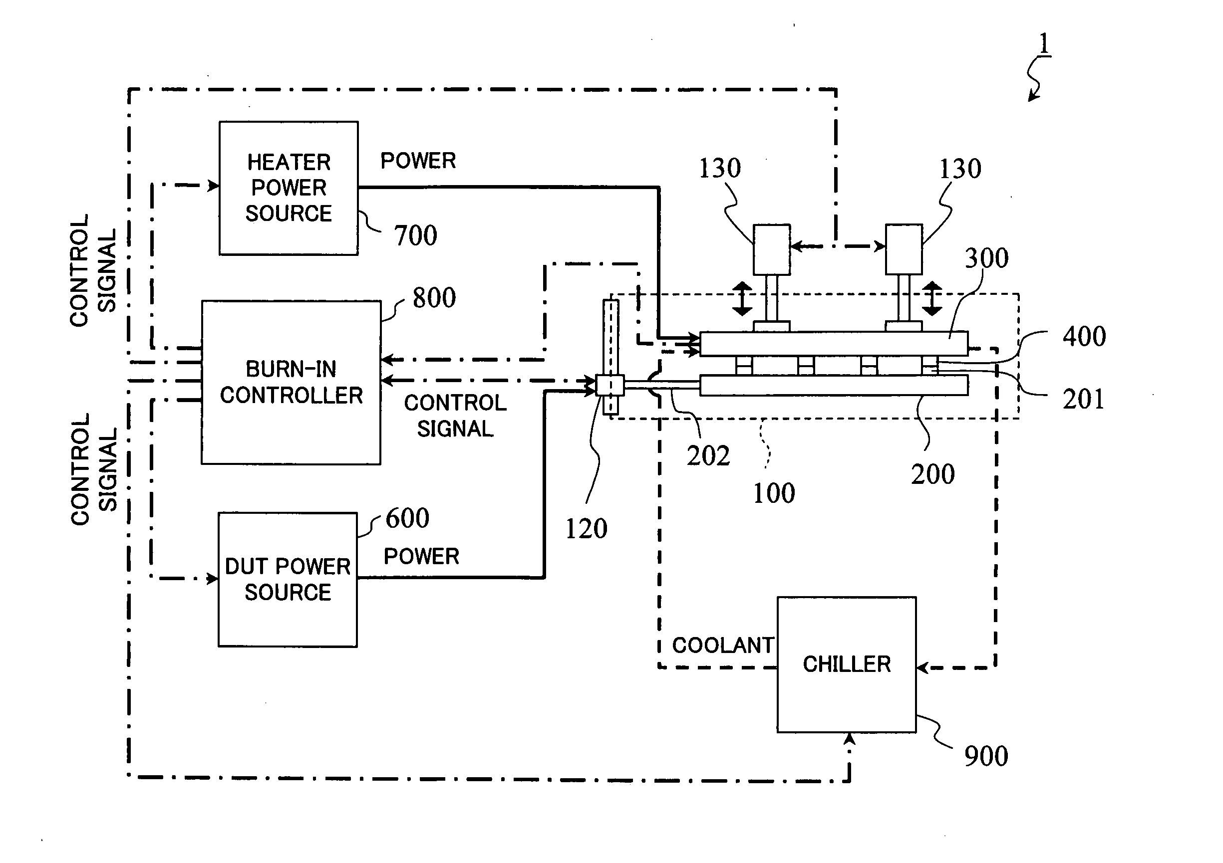
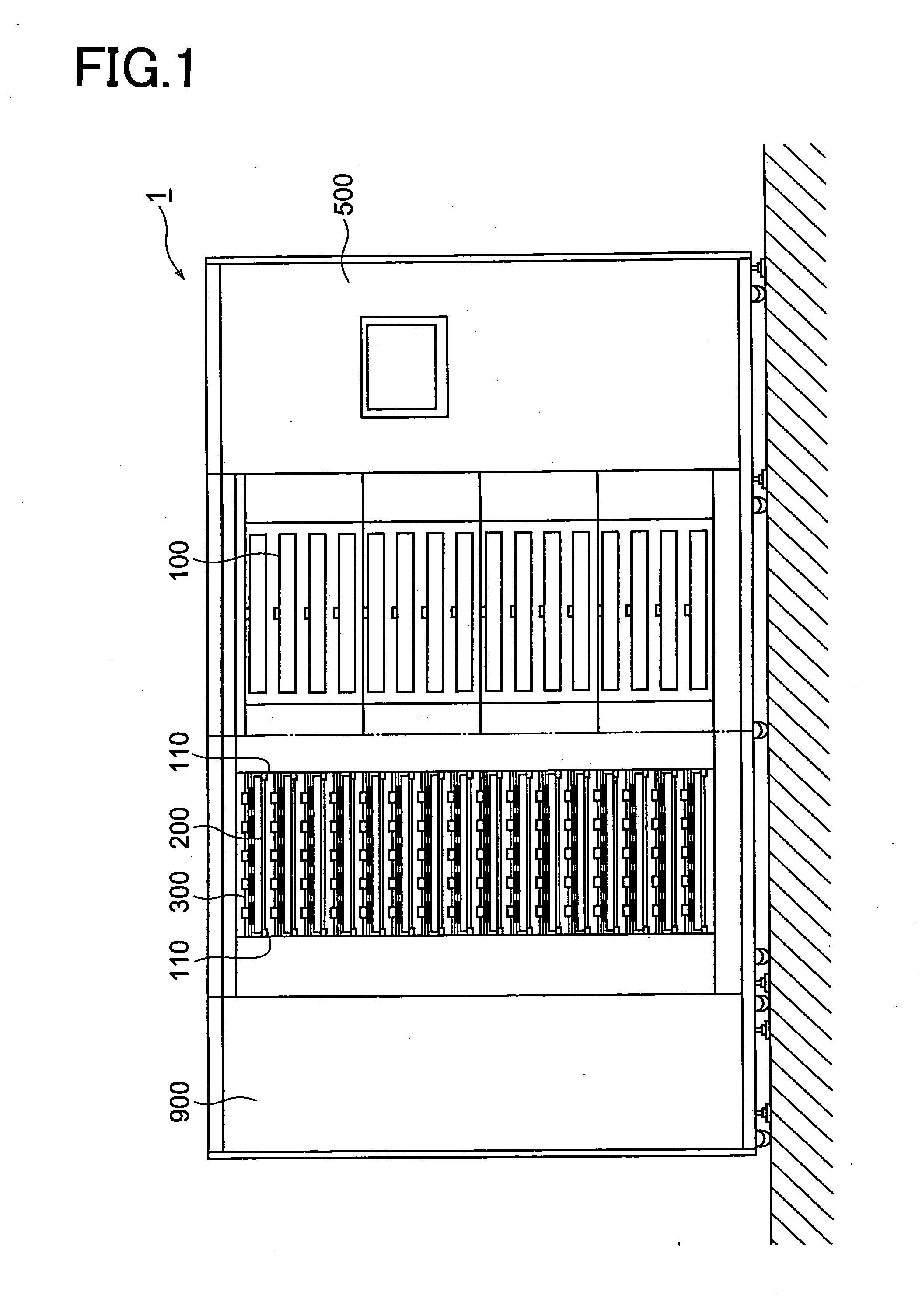
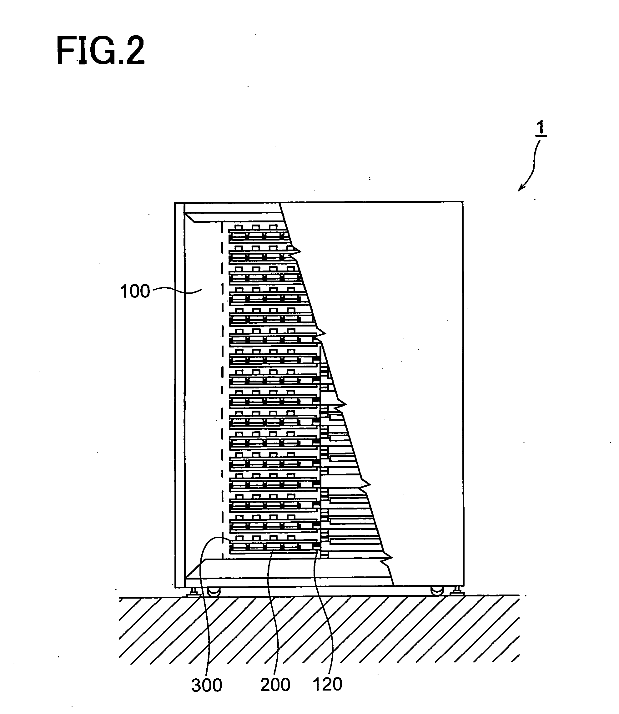
[0072]FIG. 1 is a front view of an overall burn-in system according to a first embodiment of the present invention, FIG. 2 is a side view of the overall burn-in system shown in FIG. 1, FIG. 3 is a conceptual view of the system configuration of the burn-in system shown in FIG. 1, and FIG. 4 is a plan view of an overall burn-in board mounting DUTs in the first embodiment of the present invention.
[0073] First, explaining the overall configuration of the burn-in system 1 according to the first embodiment of the present invention, this burn-in system 1, as shown in FIG. 1 to FIG. 3, is provided with a burn-in chamber 100 which can hold burn-in boards 200 on which for example DUTs (devices under test) such as IC chips (corresponding to “device under test” in the claims) are mounted and has temperature adjustment boards 300 with temperature adjustment heads 400 for adjusting the DUTs in temperature arranged facing the burn-in boards 200; a DUT power source 600 for supplying the DUTs with ...
second embodiment
[0144]FIG. 17 is a side view of a temperature adjustment head in a second embodiment of the present invention.
[0145] The burn-in system according to the second embodiment of the present invention differs in structure of the temperature adjustment head from the burn-in system 1 according to the first embodiment, but the rest of the configuration is identical to that of the burn-in system 1 according to the first embodiment. Below, the burn-in system according to the second embodiment will be explained only with reference to the points of difference from the burn-in system 1 according to the first embodiment.
[0146] The temperature adjustment head 400′ in the present embodiment, as shown in FIG. 17, is not provided with any heater block. Instead, a bypass 414′ of the cooling block 410′ is provided with a valve 417′ (variable flow rate means). The head differs from the first temperature adjustment head 400a in the first embodiment on this point, but otherwise is the same in configurat...
third embodiment
[0150]FIG. 18 is a side view of a temperature adjustment head in a third embodiment of the present invention, FIG. 19 is a bottom plan view of the temperature adjustment head shown in FIG. 18, and FIG. 20 is a schematic view of a coolant recovering means of a burn-in system according to a third embodiment of the present invention.
[0151] In the burn-in systems according to the first and second embodiments explained above, the DUTs were indirectly cooled by coolant through the cooling blocks so as to adjust the DUTs in temperature, but in the burn-in system according to the third embodiment of the present invention, the coolant is made to directly contact the DUTs to adjust the DUTs in temperature.
[0152] Therefore, the burn-in system according to the third embodiment of the present invention differs in the structure of the temperature adjustment heads. Further, it differs from the burn-in system 1 according to the first embodiment in the point of being provided with coolant recoveri...
PUM
 Abstract
Description
Claims
Application Information