Chip inductor

a chip and inductor technology, applied in the direction of transformer/inductance details, inductance, core/yokes, etc., can solve the problem of hard magnetic saturation of the plate member, achieve excellent direct-current superposition characteristics, reduce size or height, and prevent magnetic leakage

Inactive Publication Date: 2007-03-22
SUMIDA CORP
View PDF6 Cites 35 Cited by
  • Summary
  • Abstract
  • Description
  • Claims
  • Application Information

AI Technical Summary

Benefits of technology

[0017] According to the present invention, it is possible to provide a chip inductor capable of effectively preventing a magnetic leakage and having excellent direct-current superposition characteristics and having an advantage in reducing in size or height.

Problems solved by technology

For this reason, even if the plate member containing the iron-based amorphous powder is reduced in thickness, the plate member is hard to magnetically saturate.

Method used


Image

  • Chip inductor
  • Chip inductor
  • Chip inductor

Examples


Embodiment Construction

[0021] Hereinafter, an embodiment of a chip inductor according to the present invention will be described with reference to the drawings.

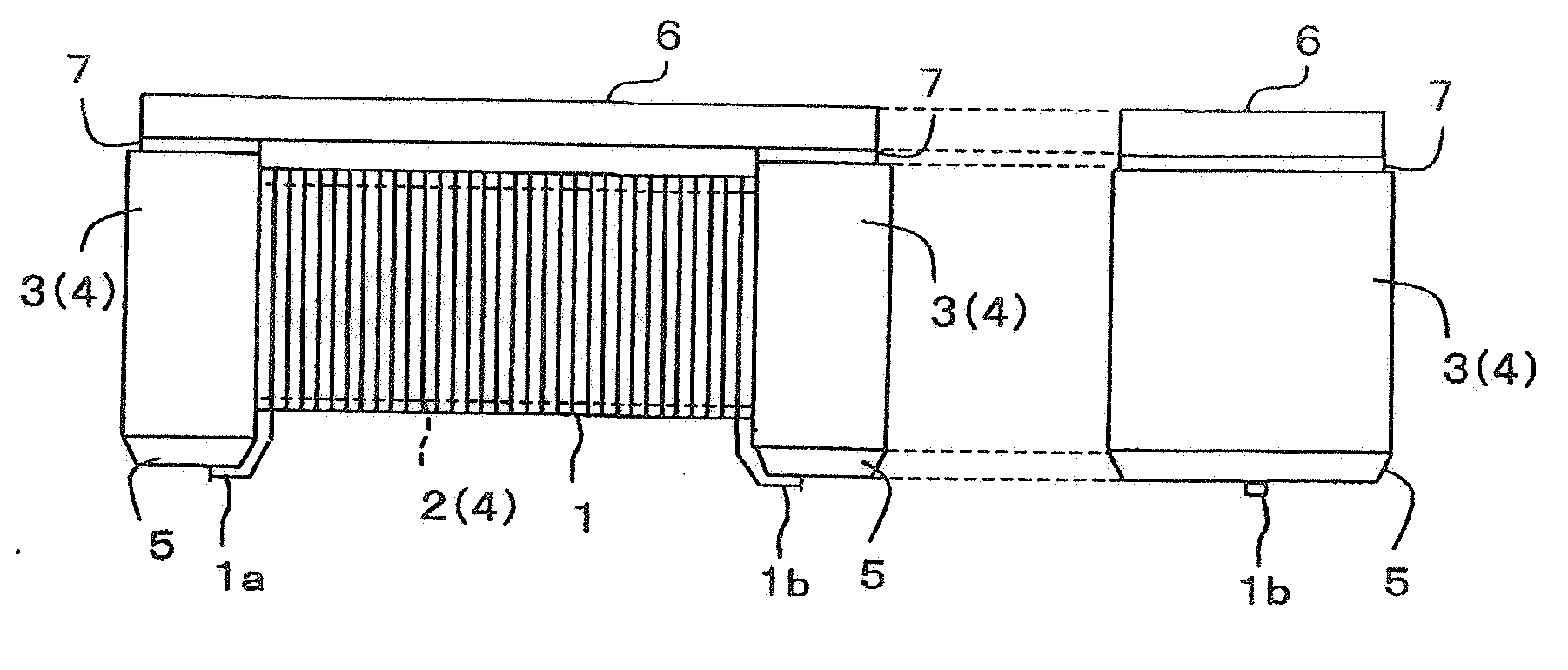
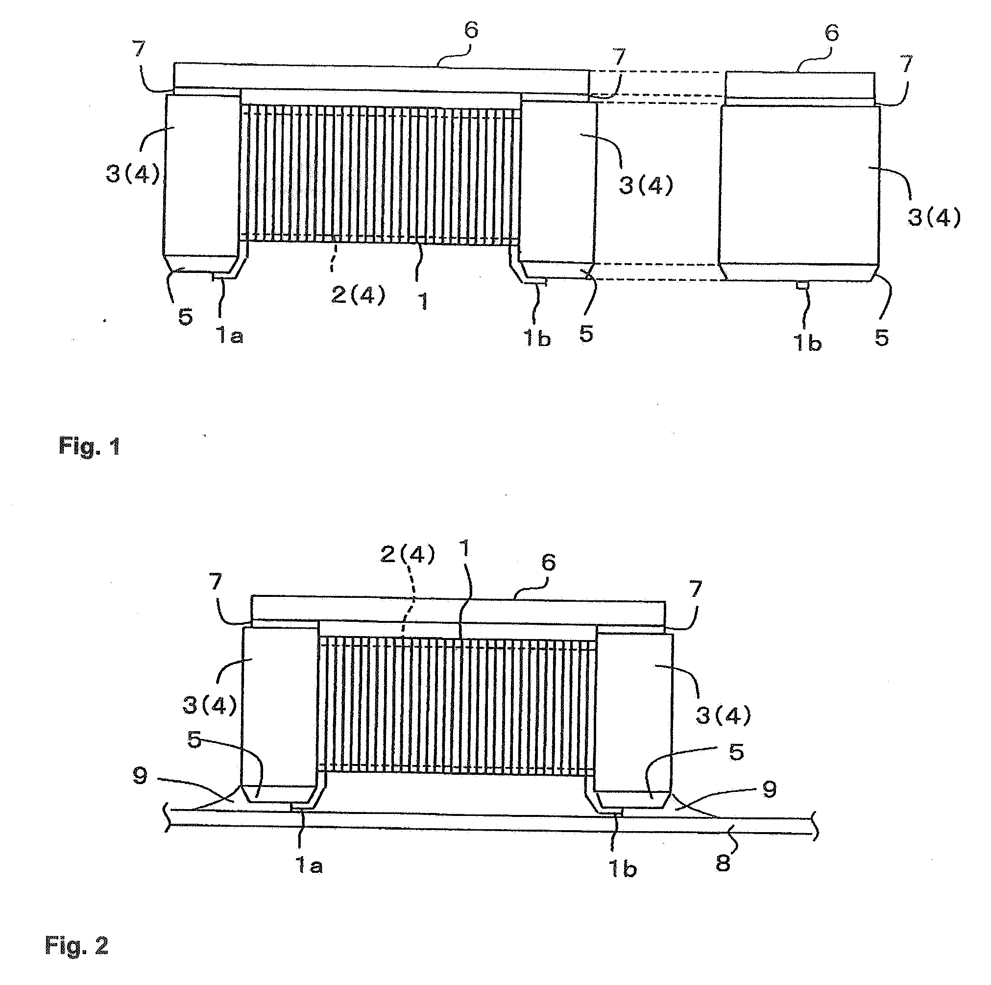
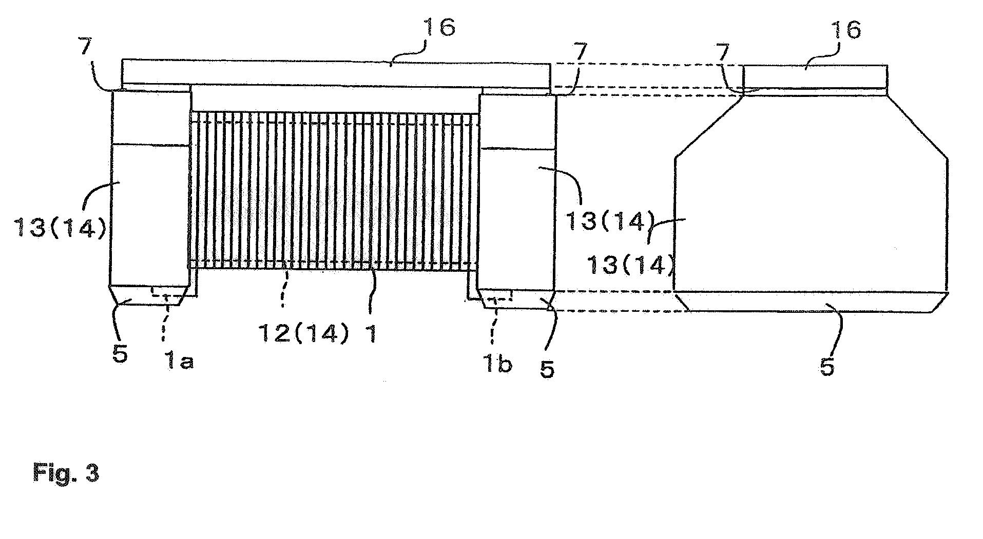
[0022]FIG. 1 is a side view of a chip inductor according to an embodiment of the present invention.

[0023] The chip inductor according to this embodiment includes a winding 1 and a drum core 4 having a winding shaft 2, around which the winding 1 is wound, and flange parts 3, 3 formed on both end portions in the direction of length of the winding shaft 2. In FIG. 1, the reference numerals of the drum core 4 are shown in parentheses after the respective reference symbols of the winding shaft 2 and the flange parts 3, 3.

[0024] The winding shaft 2 is formed in the shape of a nearly quadrangular prism. The flange parts 3, 3 are plate-shaped members each formed in the shape of a nearly quadrangular prism having a larger area than the cross section in the axial direction of the winding shaft 2. In the flange parts 3, 3, the length of one side of a plane...


PUM

PropertyMeasurementUnit
average grain diameteraaaaaaaaaa
grain diameteraaaaaaaaaa
sizeaaaaaaaaaa

Abstract

A chip inductor includes: a winding; a ferrite-based drum core having flange parts on both ends of a winding shaft around which the winding is wound; electrodes fixed to the flange parts on both ends of the winding shaft and for electrically connecting both ends of the winding to a mounting board; and a magnetic shield plate for connecting both flange parts in a region other than the electrodes wherein the magnetic shield plate is a plate member containing an iron-based amorphous powder.

Description

CLAIM OF PRIORITY [0001] This application claims the benefit of Japanese Patent Application No. 2005-273559 filed on Sep. 21, 2005, the entire contents of which are hereby incorporated by reference herein. BACKGROUND OF THE INVENTION [0002] 1. Field of the Invention [0003] The present invention relates to a chip inductor of a surface mounting type used for electronic devices and the like. [0004] 2. Description of the Related Art [0005] In recent years, as progress has been made in reducing the size and thickness of electronic devices typified by a mobile phone and a notebook-type PC, there has been an increasing demand for reducing the size and height of a chip inductor for surface mounting that occupies a comparatively large volume in an electronic component mounted on a circuit board. [0006] By reducing the size and height of the chip inductor for surface mounting, the structure of the chip inductor and a method for mounting the chip inductor on a circuit board have been improved....

Claims


Application Information

Patent Timeline
Patent Type & Authority Applications(United States)
IPC IPC(8): H01F27/02
CPCH01F3/10H01F27/34H01F27/292H01F17/045H01F1/37B82Y25/00
Inventor WATANABE, YOSHITO
Owner SUMIDA CORP
Why Eureka
Try Eureka