However, this also causes adhesion between the resin material and a surface of a mold for resin molding to be increased.
Therefore, there is a problem that mold release characteristics in removing the molded product from the mold after the resin-seal-molding are deteriorated and the molded product cannot be released efficiently.
Additionally, for example if molded product releasing means for releasing the molded product by forcibly ejecting the molded product with an ejector pin or the like is employed, coupled with the compactness of the molded product, there is a problem that the molded product body (resin-seal-molded body) may be damaged and a crack may occur, or it may be broken and its quality may be degraded.
Further, when an ejector pin mechanism such as described above is incorporated into a resin-molding mold, there is a problem that the mold structure becomes complicated and the overall durability is impaired.
Still further, when a mechanism for melting the resin material or a mechanism for transferring the molten resin material is incorporated inside a mold, not only the mold structure becomes complicated but also there is a problem that resin-seal-molding conditions become limited based on the complicated mold structure.
However, the effect of the surface treatment is not uniform, and it is less durable.
Therefore, clamping state is not uniform among the large substrates even if the large substrates are simultaneously applied with mold-clamping pressure.
This sometimes causes part of the resin material to flow into between each of the large substrates and the mold surfaces, resulting in formation of resin flash on the
substrate surface and on the mold surface.
Conversely, if each of the substrates is applied with the clamping pressure so as to prevent the resin flash formation, there is an
adverse effect that semiconductor elements or interconnections on the substrates are damaged if the clamping pressure is excessive.
Thus, the variation in the thicknesses of substrates has been a factor of significant degradation in the quality of a molded product.
Based on such a mold structure, the following problem on the resin-seal-molding arises.
Accordingly, the molten resin material in the pot or in the resin path in the state described above is prone to enter a gap on the mold face than the material in other sites because of the resin pressure.
As a result, such an
adverse effect arises that a thin resin flash is formed on the mold face near the pot portion and the resin path portion.
Setting of resin-seal-molding conditions, setting of the mold
surface shape or manufacturing of the mold for preventing such an
adverse effect is extremely cumbersome.
In addition, considering for example setting of resin-seal-molding conditions specific to the resin material used in the resin-seal-molding, there is a problem that the overall working efficiency is significantly impaired.
Further, such a thin resin flash is difficult to be completely removed in the cleaning step.
Thus, there is a problem that it mixes into the molten resin material in the next resin-seal-molding, resulting in a defective product.
There is also a problem that the cured resin flash causes failure in clamping in the clamping step.
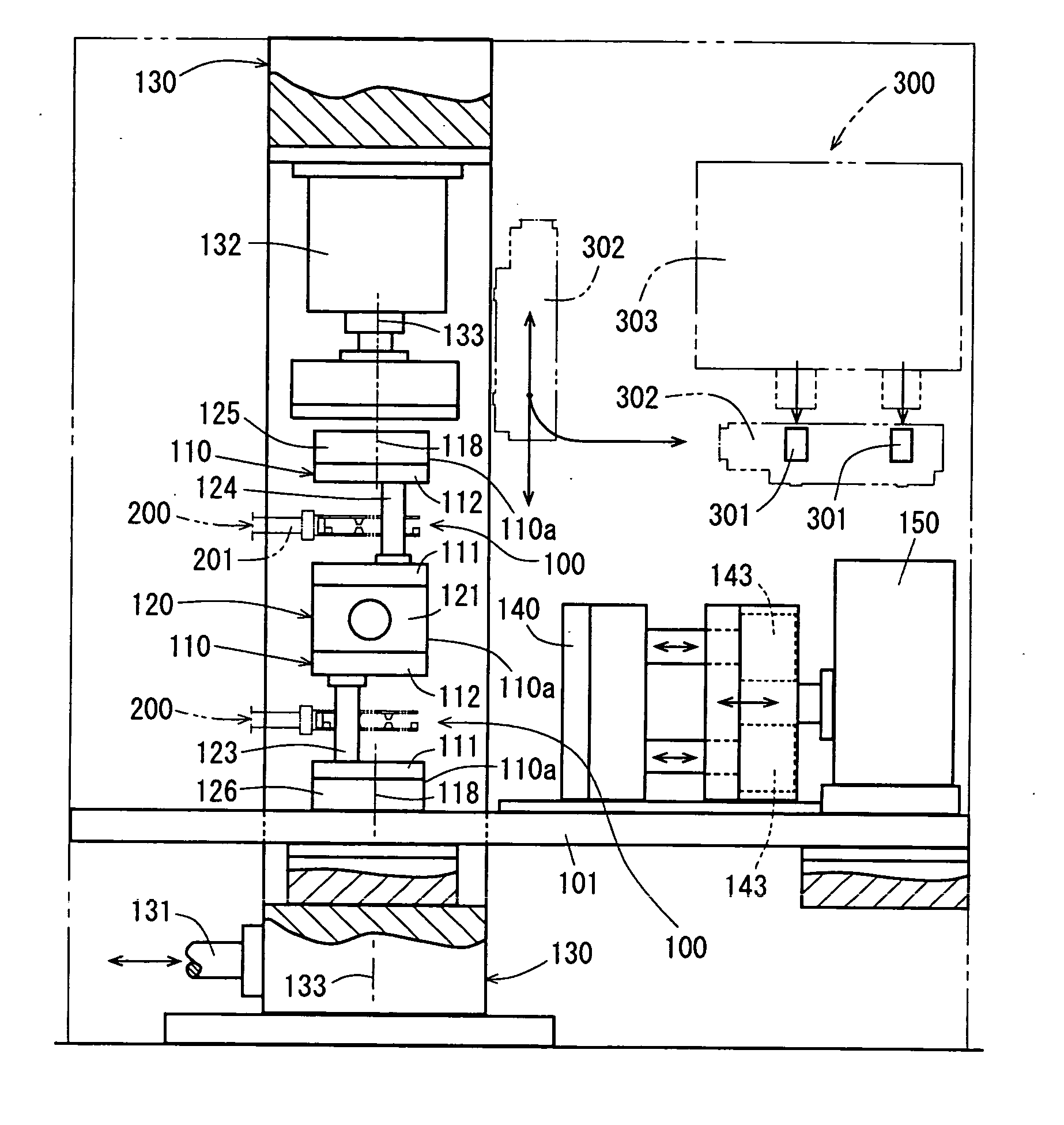
Among the conventional resin-seal apparatuses wherein many substrates are mounted on one mold structure to carry out the resin-seal-molding, the apparatus employing the floating structure for solving the aforementioned problem of variation in a substrate (Japanese Patent Laying-Open No. 11-126787, (page 7, FIG. 1) not only introduces further complication into a general mold structure, but also involves a problem of cumbersome mold manufacturing associated with an increase in costs.
Works of adjusting elastic pressing force on each site of the substrate, works of adjusting elastic pressing force when performing resin-seal-molding to other type of substrate having different thickness and the like are cumbersome.
Additionally, when resin-seal-molding electronic components while many substrates are supply-set to the mold face (PL face), coupled with the fact that each substrate varies in thickness, works such as adjusting the elastic pressing force on each substrate is substantially impossible.
Further, works such as mold maintenance is very cumbersome.
Accordingly, it is difficult to bring the resin-seal-molding apparatus having the floating structure into practical use.
Further, the amount of resin cured in this site (the amount of resin to be wasted) is great and is not economical.

