Cascode switch power supply

a power supply and switch technology, applied in the field of analog integrated circuits and switching semiconductor circuits, can solve the problems of reducing current consumption, insufficient voltage to maintain the vcc terminal of the control circuit above its lower undervoltage, and waste of considerable energy, so as to reduce power and reduce power

Active Publication Date: 2007-03-29
DIALOG SEMICONDUCTOR GMBH
View PDF4 Cites 74 Cited by
  • Summary
  • Abstract
  • Description
  • Claims
  • Application Information

AI Technical Summary

Benefits of technology

[0033] It is an object of this invention to produce a circuit which switches a power MOSFET with a minimum of required power. It is a further object of this invention to provide a means to significantly reduce power loss under the condition of no load at the power supply output.
[0034] It is a further object of this invention to provide a scheme for generating an efficient low voltage source of power for the control chip of a power supply control circuit, and to do so with a minimum of components and cost.
[0036] The present invention allows a mains powered switching power supply to require a significantly reduced power for the driving of a power device, and to generate the control power without need for a separate transformer winding dedicated to this purpose. The use of a common gate power MOSFET eliminates the need for a DC power source to drive the gate capacitance, and the common gate connection additionally allows for the implementation of a charge-pump conversion of switching energy to provide power for control circuitry. Because this charge pump conversion is frequency dependent, the present invention utilizes this charge pump as a means to trigger a power cycling mode to significantly reduce power at no-load conditions.

Problems solved by technology

Considering the number of these devices in use, and the fact that they are rarely if ever unplugged from the mains, a considerable amount of energy is wasted.
The resultant voltage is insufficient to maintain the VCC terminal of the control circuit above its lower undervoltage lockout threshold.
One difficulty of implementing the burst mode operation with the scheme shown in FIG. 2 is that the auxiliary power rail 10 and the output voltage at terminal 6 are cross-regulated, that is, the two voltages are both based upon the peak voltages across two coupled winding.
A limiting factor in reducing the current consumption is the current needed for driving the gate of switch 2.
The construction of high voltage devices requires a significant increase in size compared to similar low voltage devices.

Method used


Image

  • Cascode switch power supply
  • Cascode switch power supply
  • Cascode switch power supply

Examples


Embodiment Construction

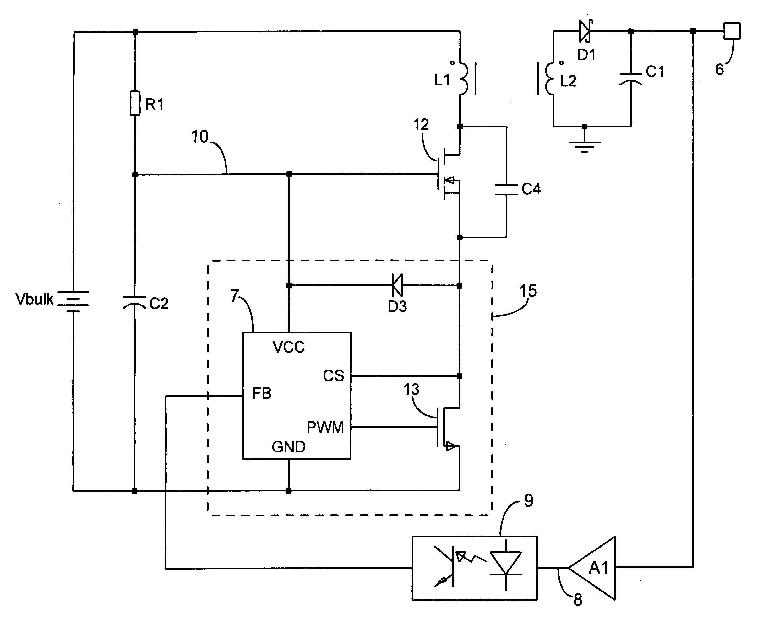
[0044] A preferred embodiment of the present invention is shown in FIG. 6. A bulk supply voltage, Vbulk, represents the incoming energy source, typically rectified AC mains but alternately a DC source as is generally used in telecom systems. A control circuit 7 has the conventional function of controlling a pulse modulated signal at the PWM terminal as a function of the inputs to the control circuit at the CS and FB terminals. Control circuit 7 receives its required power from a VCC terminal connected to an auxiliary power supply rail 10.

[0045] The PWM output of the control circuit 7 drives a low voltage transistor 13, which also acts as a current sense element. When MOSFET 13 is in its “on” state, it has a resistive characteristic and can be seen in this state as analogous to current sense element 4 of FIGS. 1, 2, 4 and 5. The current sense circuitry of control circuit 7 must gate the voltage at the CS input as it is a valid representation of switch current only when MOSFET 13 is ...


PUM


Abstract

A switching power supply is disclosed for improving the no-load power drain of low-power mains operated supplies. The power converter utilizes a cascoded switch arrangement with a conventional high voltage power MOSFET and a low voltage, low gate charge MOSFET. Driving only the small low voltage device reduces the power required for gate drive. The disclosed configuration is also capable of generating a non-isolated auxiliary rail for powering its control circuitry utilizing the parasitic capacitance of the high voltage power devices as an element in a charge pump. The resulting power supply requires significantly fewer components.

Description

CROSS REFERENCE TO RELATED APPLICATION [0001] This application claims the benefit of prior U.S. Provisional Application Ser. No. 60-720,617 titled “LOW POWER LOSS OFFLINE POWER CONVERSION.”BACKGROUND OF THE INVENTION [0002] 1. Field of the invention [0003] The present invention is in the field of electronic circuits. The present invention is further in the field of analog integrated circuits and switching semiconductor circuits. [0004] The invention also falls within the field of switching power converters that convert one DC level to another or convert AC power to DC power. [0005] 2. Brief Description of Related Art [0006] The desire to lower overall energy and the proliferation of small low power and mobile devices has created new requirements of offline power supplies. Consumer electronics are often supplied with no internal power supply, and instead are powered by an external “wall wart”, a small power supply typically built directly into the AC mains plug. Traditionally made fr...

Claims


Application Information

Patent Timeline
Patent Type & Authority Applications(United States)
IPC IPC(8): H02M3/335
CPCH02M3/33523H02M2001/0006H02M3/33569H02M1/088H02M1/0006H02M1/0009
Inventor SAWTELL, CARL K.
Owner DIALOG SEMICONDUCTOR GMBH
Why Eureka
Try Eureka