Inspection device and inspection method for active matrix panel, and manufacturing method for active matrix organic light emitting diode panel

a technology of active matrix and inspection method, which is applied in the direction of semiconductor/solid-state device testing/measurement, identification means, instruments, etc., can solve the problems of inability to conduct an electric current on the driving tft only by input and output, inability to inspect open/short defects in the driving tft, and inability to perform open/short measurement of the driving

Inactive Publication Date: 2007-04-05
INT BUSINESS MASCH CORP
View PDF5 Cites 135 Cited by
  • Summary
  • Abstract
  • Description
  • Claims
  • Application Information

AI Technical Summary

Benefits of technology

[0014] Still another aspect of the present invention realizes calculation of unevenness in Von−Vcff values in normally operating pixels within a panel and thereby to estimate accuracy of formation of pixel circuits.
[0019] Moreover, the on-state parasitic capacitance measuring means estimates the parasitic capacitance on each line of the inspection wiring constituting the active matrix panel while setting the driving TFT of a pixel subjected to AC coupling directly with the relevant line of the inspection wiring to an on state. Meanwhile, the off-state parasitic capacitance measuring means estimates the parasitic capacitance on each line of th inspection wiring constituting the active matrix panel while setting the driving TFT of the pixel subjected to AC coupling directly with the relevant line of the inspection wiring to an off state. Moreover, the inspecting means can estimate the number of the pixels having open / short defects in the driving TFTs thereof by use of a difference between maximum / minimum values of the estimated parasitic capacitance and the individual parasitic capacitance.

Problems solved by technology

Although there are at least two TFTs in the pixel circuit of the TFT array substrate in the AMOLED, it is impossible to conduct an electric current on the driving TFT only by input and output from a panel interface terminal.
Accordingly, it is not possible to inspect open / short defects in the driving TFT 302 only by input and output to / from the panel interface erminal.
As a result, it is not possible to perform open / short measurement of the driving TFT 302 set to the open-drain (or open-source) state by use of the known techniques.
However, this technique is not designed to perform inspection after patterning the pixel electrodes.
Therefore, this technique cannot inspect defects which are attributable to patterning.
Moreover, although this technique can inspect a defect of the driving TFT 302, the technique cannot specify a type of such a defect (whether the defect is an open defect or a short defect).
As a result, this technique cannot count the number of bright points or dark points (dead points), which are defects of a display device after formation of the OLED 301, or obtain data corresponding to an evaluation standard set up by an inspector, for example.

Method used


Image

  • Inspection device and inspection method for active matrix panel, and manufacturing method for active matrix organic light emitting diode panel
  • Inspection device and inspection method for active matrix panel, and manufacturing method for active matrix organic light emitting diode panel
  • Inspection device and inspection method for active matrix panel, and manufacturing method for active matrix organic light emitting diode panel

Examples


Embodiment Construction

[0043] Now, the present invention will be described in detail based on an embodiment with reference to the accompanying drawings.

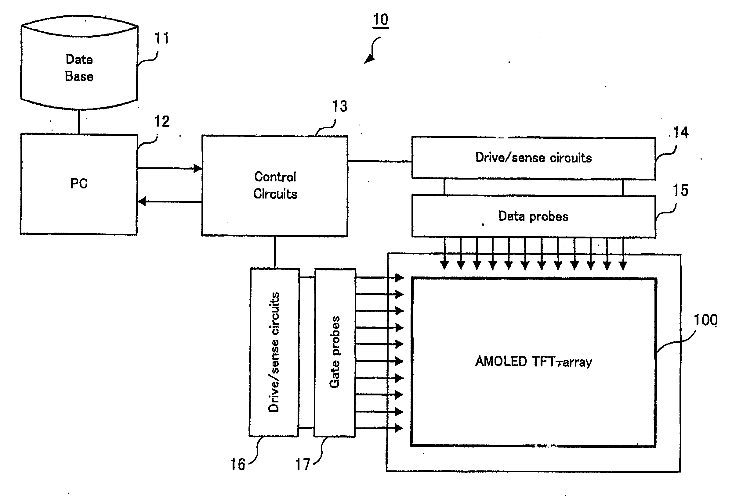
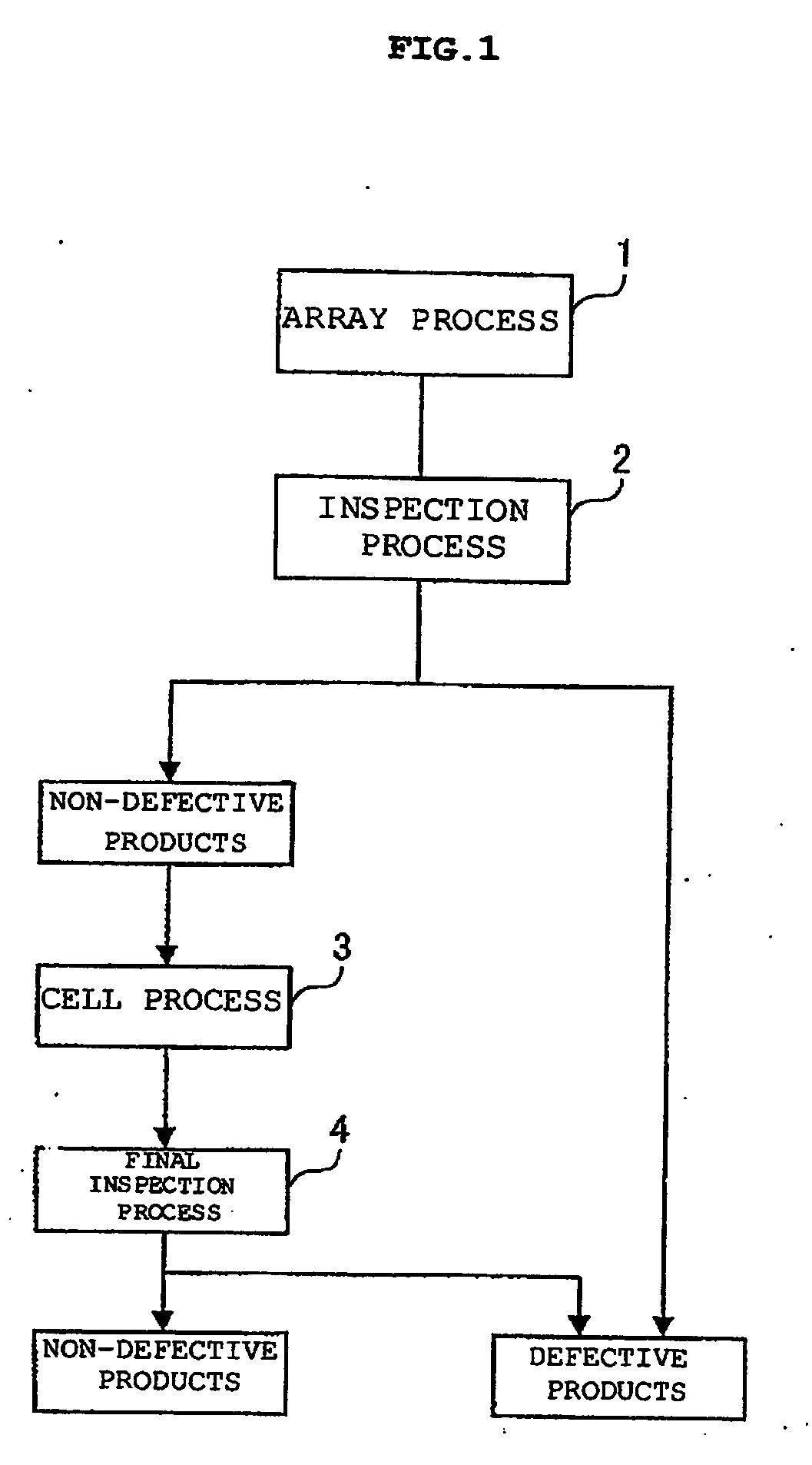
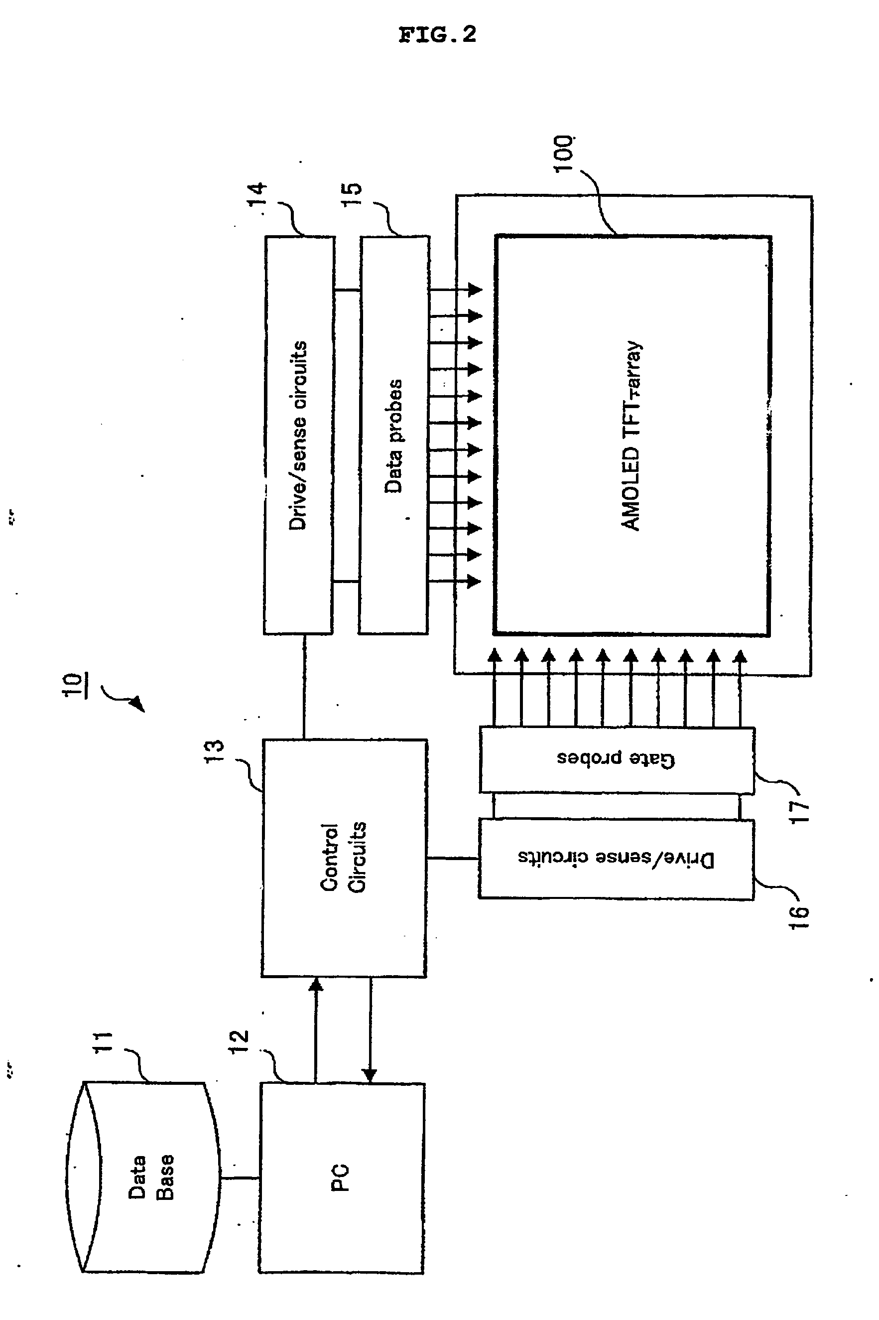
[0044]FIG. 1 is a view for explaining a manufacturing process of an OLED panel in accordance with an embodiment of the present invention. The manufacturing method includes an array process 1 of fabricating a thin film transistor (TFT) array (an active matrix panel) which is a driving circuit for the OLED, and an inspection process 2 of carrying out a performance test on the independent TFT array thus fabricated. The inspection process 2 checks whether open / short defects of wiring are below a a predetermined condition and whether characteristics of the driving TFTs constituting the TFT array are uniform throughout the panel. A TFT array judged as a defective product in this inspection process 2 will not be forwarded to a subsequent process but removed instead. A TFT array judged as a non-defective product will be forwarded to a cell process 3 of forming th...


PUM


Abstract

An inspection method includes an array process of forming a TFT array on a substrate to fabricate an active matrix panel, an inspection process of carrying out a performance test on the fabricated active matrix panel, and a cell process of mounting an OLED on the active matrix panel after the inspection process. In the inspection process, variation in parasitic capacitance through a pixel electrode is measured when driving TFTs constituting the active matrix fabricated in the array process are turned on and when the driving TFTs are turned off, and open / short defects in the driving TFTs are thereby inspected.

Description

[0001] This application is a divisional of its parent application having Ser. No. 10 / 848,318, filed May 18, 2004.FIELD OF THE INVENTION [0002] The present invention relates to an inspection device and the like for an active matrix organic light emitting diode (OLED) panel, and more specifically to an inspection device and the like for conducting performance inspection of a thin film transistor (TFT) array prior to an OLED formation process. BACKGROUND [0003] An OLED (also referred to as organic electro luminescence (EL)) is for conducting a direct current on a fluorescent organic compound which is excited by application of an electric field, and thereby causing light emission of the compound. The OLED is drawing attention as a next-generation display device in terms of low-profileness, a wide view angle, and a wide gamut, etc. Whereas a driving method for the OLED includes a passive type and an active type, the active type is suitable for achieving a large-screen and high-definition...

Claims


Application Information

Patent Timeline
Patent Type & Authority Applications(United States)
IPC IPC(8): G01R31/00H05B33/10G01R27/26G01R31/26G09F9/00G09F9/30G09G3/00G09G3/32H01L21/66H01L27/32H01L29/786H01L51/50H05B33/14
CPCG09G3/006G09G3/3225G09G2300/0842G09G2330/10
Inventor NAKANO, DAIJUSAKAGUCHI, YOSHITAMI
Owner INT BUSINESS MASCH CORP
Why Eureka
Try Eureka