Efficient provision of alignment marks on semiconductor wafer

a technology of alignment marks and semiconductors, applied in semiconductor/solid-state device testing/measurement, semiconductor/solid-state device details, instruments, etc., can solve the problems of increasing manufacturing costs, affecting and affecting the efficiency of alignment marks, so as to improve the yield of semiconductor devices and widen the width of scribe lines

Inactive Publication Date: 2007-04-05
RICOH ELECTRONIC DEVICES CO LTD
View PDF1 Cites 11 Cited by
  • Summary
  • Abstract
  • Description
  • Claims
  • Application Information

AI Technical Summary

Benefits of technology

[0026] When the device chip areas included in each one of the multi chip areas are arranged such as to include two or more device chip areas in the X-axis direction and three or more device chip areas in the Y-axis direction, and three alignment marks are situated at positions corresponding to three respective apexes of a right-angle triangle, there is no need to dispose the alignment marks around each and every single one of the device chip areas, so that the alignment marks can be arranged without widening the width of the scribe lines. Since each multi chip area includes two alignment marks arranged in the X-axis direction and two alignment marks arranged in the Y-axis direction, these three alignment marks can be utilized to perform positioning and angle alignment of the semiconductor wafer.
[0027] When the device chip areas included in each one of the multi chip areas are arranged such as to include two or more device chip areas in the X-axis direction and three or more device chip areas in the Y-axis direction, and four alignment marks are situated at positions corresponding to four respective corners of a rectangle comprised of two straight lines extending in the X-axis direction and two straight lines extending in the Y-axis direction, unavailability of one of the alignment marks due to its defective shape or the like is recoverable since the remaining alignment marks can be utilized to perform positioning and angle alignment of the semiconductor wafer. With this provision, the yield of semiconductor devices can be improved.
[0028] According to at least one embodiment of the present invention, the method of determining a layout of a semiconductor wafer arranges, in an X-axis direction and a Y-axis direction on a principal surface of the semiconductor wafer, multi chip areas each including two or more device chip areas, provides scribe lines extending in the X-axis direction and in the Y-axis direction, and arrange one or more alignment marks in each of the multi chip areas on the scribe lines between adjacent ones of the device chip areas included in one multi chip area, so that the one or more alignment marks is fewer than the device chip areas in each of the multi chip areas. With this provision, there is no need to dispose the alignment marks around each and every single one of the device chip areas, so that the alignment marks can be arranged reliably even if the size of the device chip areas is small. Further, since the alignment marks are disposed between adjacent device chip areas included in one multi chip area, there is no need to arrange the alignment marks close to alignment marks provided in another multi chip area, thereby eliminating the need to widen the width of the scribe lines.
[0029] When the device chip areas included in each one of the multi chip areas are arranged such as to include one device chip area in the X-axis direction and two device chip areas in the Y-axis direction, and a number of the one or more alignment marks arranged in each one of the multi chip areas is one, there is no need to dispose the alignment marks around each and every single one of the device chip areas, so that the alignment marks can be arranged without widening the width of the scribe lines.

Problems solved by technology

This makes it difficult to dispose an alignment mark in each device chip area.
This gives rise to a problem that the manufacturing cost increases.
Further, even if an alignment mark is arranged on a scribe line, the provision of alignment marks for respective device chip areas may create interference with other cells that are arranged on scribe lines.
Because of this, there may be a situation where aliment marks cannot be disposed as desired.
This means an increase in the width of the scribe lines, resulting in a decrease in the number of device chip areas provided on a semiconductor wafer.
This gives rise to a problem that the manufacturing cost increases.

Method used


Image

  • Efficient provision of alignment marks on semiconductor wafer
  • Efficient provision of alignment marks on semiconductor wafer
  • Efficient provision of alignment marks on semiconductor wafer

Examples


Embodiment Construction

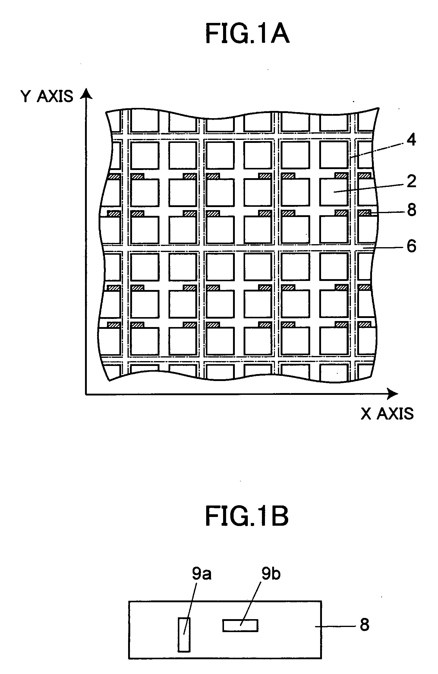
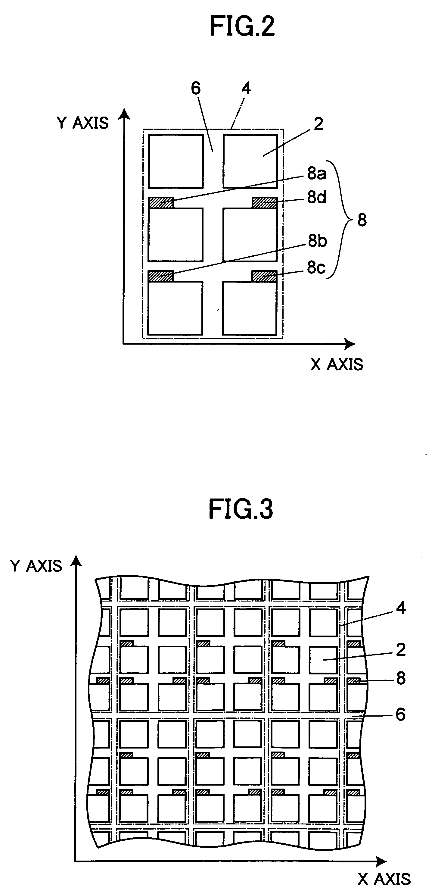
[0045] In the following, preferred embodiments of the semiconductor wafer of the present invention will be described with reference to the accompanying drawings. In the drawings referred to in this specification, the horizontal direction is referred to as an X-axis direction, and the vertical direction is referred to as a Y-axis direction. Here, the X axis and the Y axis are reference axes perpendicular to each other.

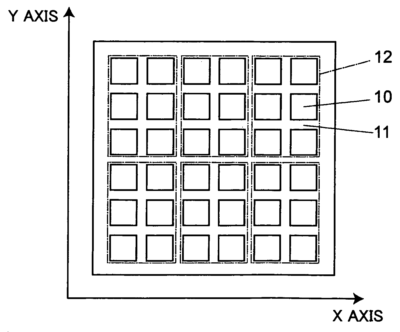
[0046]FIGS. 1A and 1B are drawings showing an embodiment of the semiconductor wafer. FIG. 1A is an enlarged view of a layout on the principal surface of the semiconductor wafer, and FIG. 1B is an enlarged view of an alignment cell. In FIGS. 1A and 1B and the drawings referred to in the following, the illustration of device chip areas 2 are intended to include an actual chip area (not shown) for use as an intended product and a guard ring (not shown) formed around the actual chip area.

[0047] On the principal surface of the semiconductor wafer, the device chip areas 2 a...


PUM


Abstract

A semiconductor wafer includes multi chip areas each including two or more device chip areas and arranged in an X-axis direction and a Y-axis direction, a plurality of scribe lines formed parallel to the X axis and the Y axis such as to separate the device chip areas from each other, and one or more alignment marks formed in each of the multi chip areas on the scribe lines between adjacent ones of the device chip areas included in one multi chip area, the one or more alignment marks being fewer than the device chip areas in each of the multi chip areas and used for positioning of the semiconductor wafer.

Description

BACKGROUND OF THE INVENTION [0001] 1. Field of the Invention [0002] The present invention generally relates to semiconductor wafers, semiconductor-wafer-layout determining methods, and reticle-layout determining methods, and particularly relates to a semiconductor wafer having an alignment mark for positioning the wafer, a semiconductor-wafer layout determining method, and a reticle-layout determining method for implementing the semiconductor-wafer layout determining method. [0003] 2. Description of the Related Art [0004] In the manufacturing of semiconductor devices having analog circuits, generally, laser trimming for adjusting resistance by cutting fuses is performed on the wafers in order to improve the analog characteristics of the semiconductor devices. An aliment mark is formed on a semiconductor wafer for the purpose of positioning the semiconductor wafer during such laser trimming process. [0005] A plurality of device chip areas are arranged in matrix form on a semiconducto...

Claims


Application Information

Patent Timeline
Patent Type & Authority Applications(United States)
IPC IPC(8): H01L21/66G01R31/26
CPCH01L23/544H01L2223/54426H01L2223/5446H01L2924/0002
Inventor SOGAWA, KOICHI
Owner RICOH ELECTRONIC DEVICES CO LTD
Why Eureka
Try Eureka