

Composite filter chip
a filter chip and composite technology, applied in the field of composite filter chips, can solve the problems of increasing the area occupied by the filter chip and the increasing area of the filter chip mounting area, and achieve the effects of reducing the area necessary, reducing the area occupied by the composite filter chip, and reducing the hermetic sealing process steps
- Summary
- Abstract
- Description
- Claims
- Application Information
AI Technical Summary
Benefits of technology
Problems solved by technology
Method used
Image

Examples
first embodiment
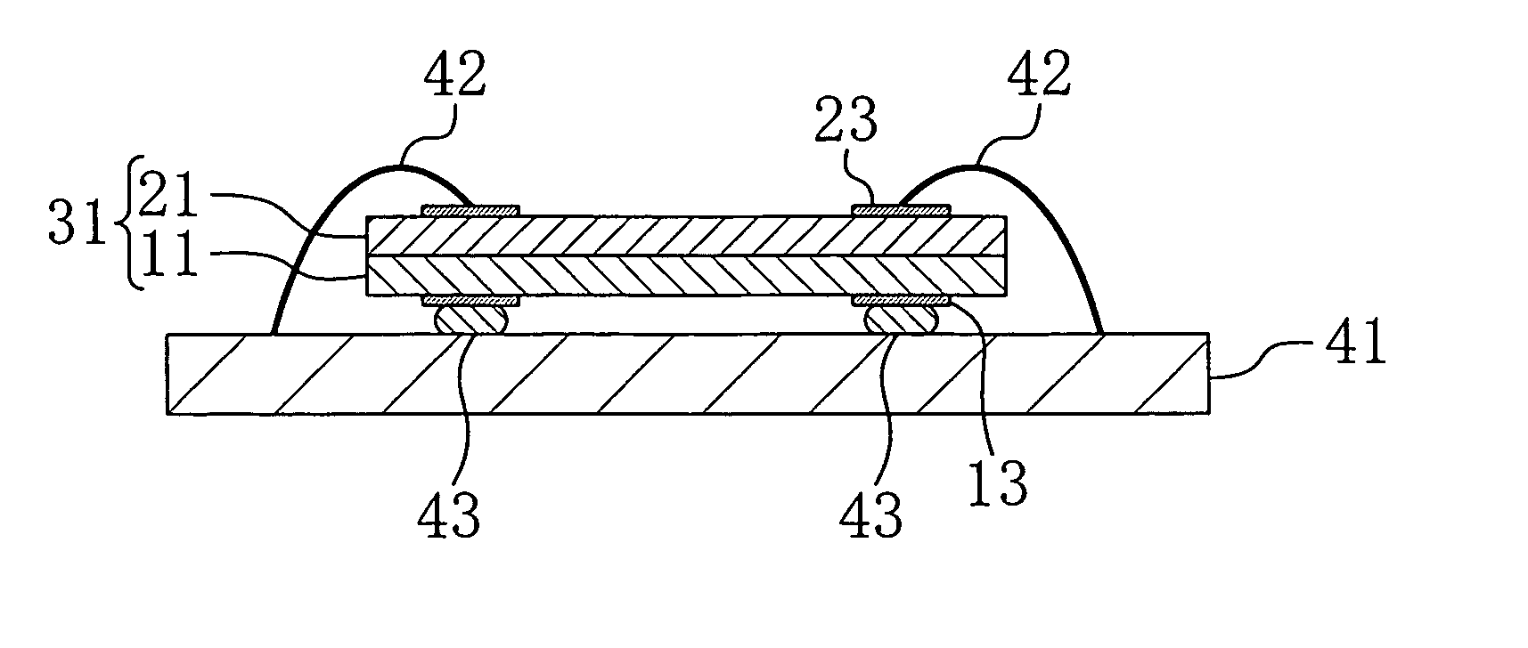
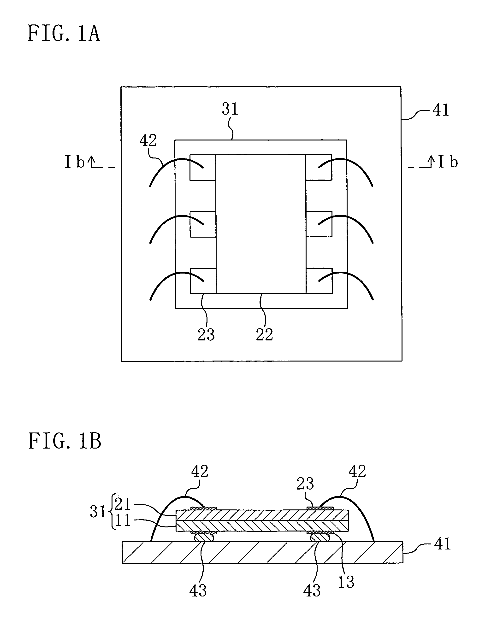
[0049] A first embodiment of the present invention will be described with reference to the accompanying drawings. FIGS. 1A and 1B illustrate a composite filter chip according to the first embodiment. FIG. 1A shows a plan structure thereof, and FIG. 1B shows a cross-sectional structure thereof taken along the line Ib-Ib in FIG. 1A.
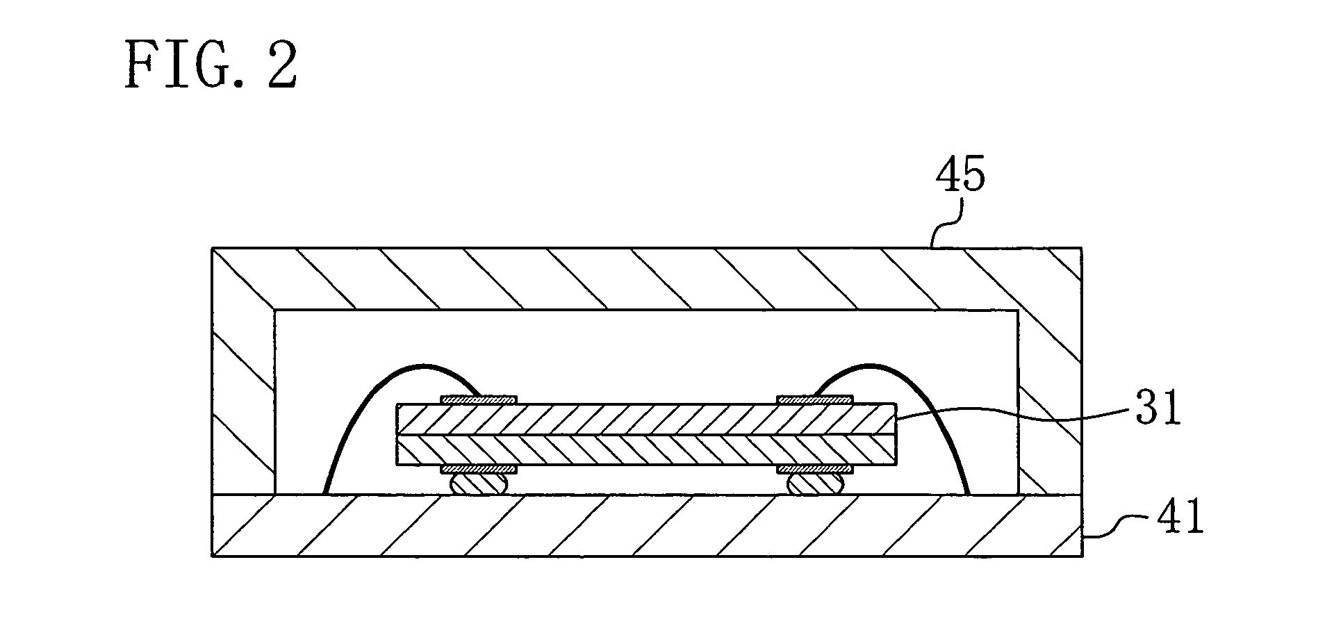
[0050] Referring to FIG. 1, the composite filter chip of the first embodiment is composed of a stacked chip 31 mounted to a mounting substrate 41. The stacked chip 31 is formed by stacking a first filter chip 11 and a second filter chip 21.
[0051] The first filter chip 11 includes: a filter circuit 12 formed on the main surface (front surface) of a substrate made of silicon; and a plurality of pads 13 formed apart from each other on both sides of the filter circuit 12. The filter circuit 12 is, for example, a filter constructed by combining a plurality of film bulk acoustic resonators (FBARs) in a ladder form. The pads 13 are electrically connected to the ...
second embodiment
[0058] A second embodiment of the present invention will be described below with reference to the accompanying drawings. FIGS. 3A and 3B illustrate a composite filter chip according to the second embodiment. FIG. 3A shows a plan structure thereof, and FIG. 3B shows a cross-sectional structure thereof taken along the line IIIb-IIIb in FIG. 3A. The description of the components shown in FIG. 3 that are the same as those shown in FIG. 1 will be omitted by retaining the same reference numerals.
[0059] The composite filter chip of the second embodiment is formed by stacking the first filter chip 11 and the second filter chip 21 with the main surfaces thereof facing each other. The first and second filter chips 11 and 21 are bonded with a sidewall member 32 interposed therebetween. The sidewall member 32 is formed to surround the perimeters of the first and second filter chips 11 and 21, and a cavity 33 is created between the first and second filter chips 11 and 21. The cavity 33 is made ...
third embodiment
[0072] A third embodiment of the present invention will be described below with reference to the accompanying drawings. FIGS. 9A and 9B illustrate a composite filter chip according to the third embodiment. FIG. 9A shows a plan structure thereof, and FIG. 9B shows a cross-sectional structure thereof taken along the line IXb-IXb in FIG. 9A. The description of the components shown in FIG. 9 that are the same as those shown in FIG. 3 will be omitted by retaining the same reference numerals.
[0073] The composite filter chip of the third embodiment is formed by stacking the first and second filter chips 11 and 21 so that the back surface of the first filter chip 11 faces the main surfaces of the second filter chip 21. The first and second filter chips 11 and 21 are stacked with the sidewall member 32 interposed therebetween. The sidewall member 32 is formed to surround the perimeters of the first and second filter chips 11 and 21, and the cavity 33 is hermetically sealed. Thereby, the fil...
PUM
 Abstract
Description
Claims
Application Information