

Printed circuit board with film capacitor embedded therein and method for manufacturing the same
- Summary
- Abstract
- Description
- Claims
- Application Information
AI Technical Summary
Benefits of technology
Problems solved by technology
Method used
Image

Examples
examples
Inventive Example
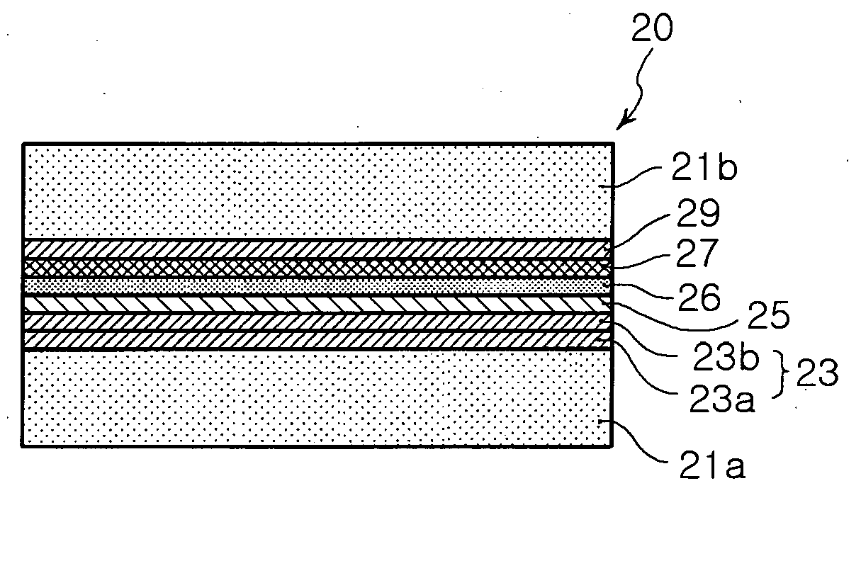
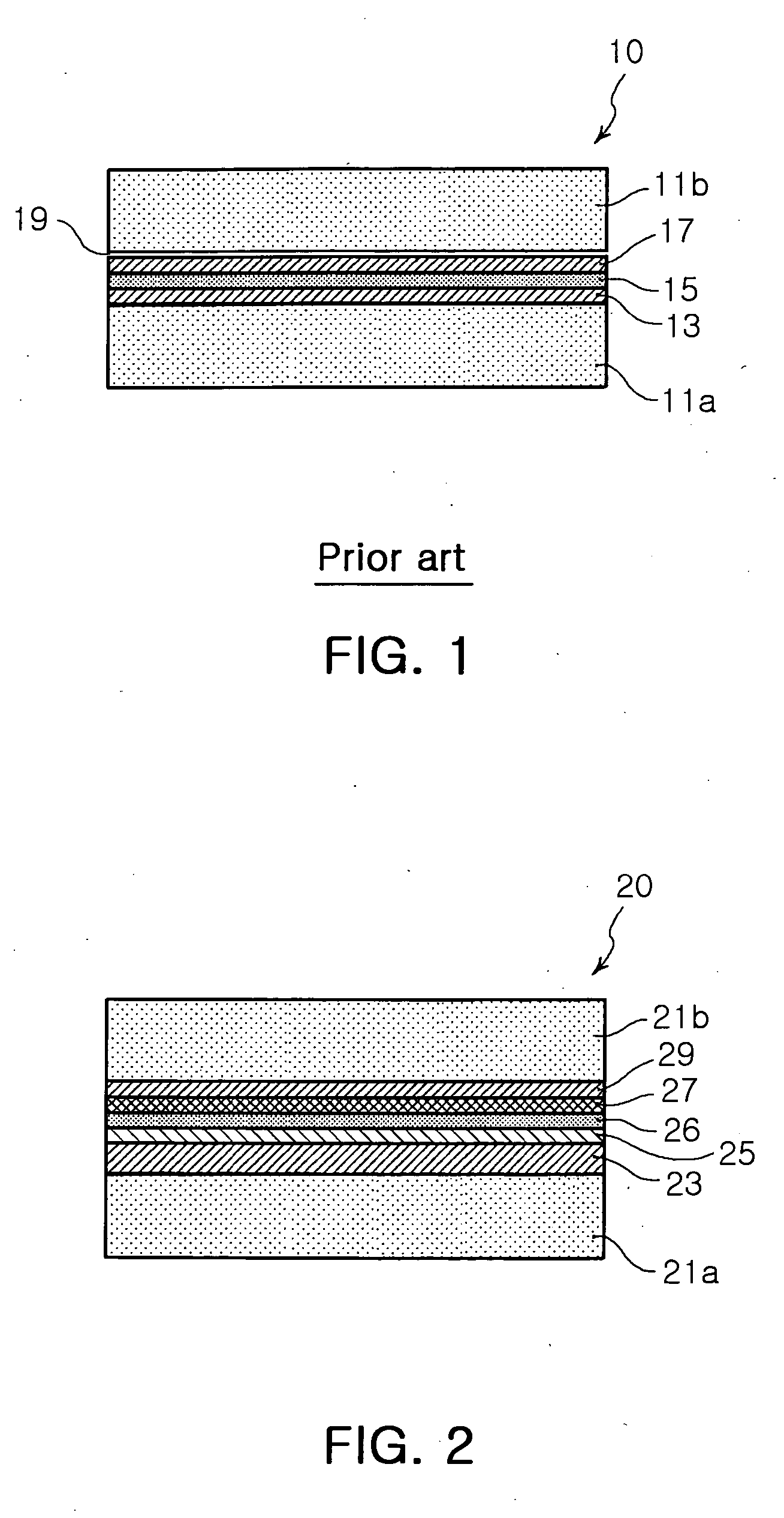
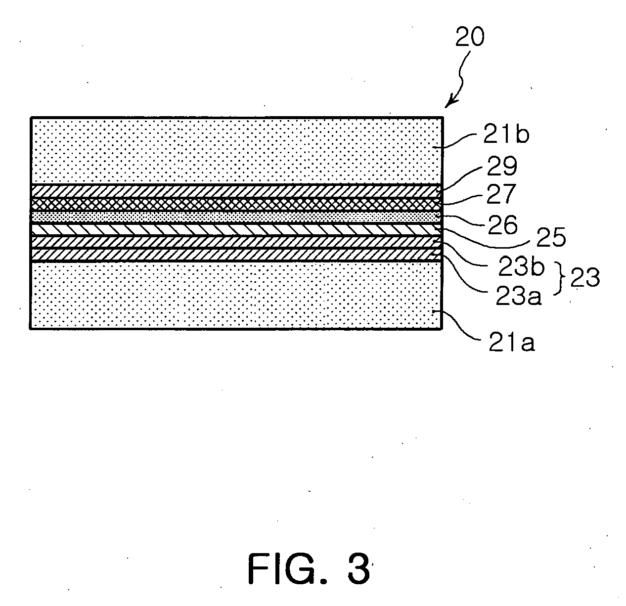
[0043] A PCB having a structure of FIG. 3 was manufactured according to the process of FIG. 4. That is, a first lower electrode was formed by plating Cu at a thickness of 1.0 μm on an epoxy-based insulating substrate via electroless plating, and a second lower electrode was formed by plating Cu at a thickness of 1.0 μm on the first lower electrode. The electrolytic plating was performed according to following conditions: current density of 1.2 A / dm2, plating time of 5 minutes, plating solution concentration of CuSO4.5H2O: 200 g / l, H2SO4: 30 g / l, Cl−: 40 ppm or less, leveler: 20 ml / l and brightener: 0.5 ml / l. Then, an amorphous paraelectric film Bi1.5ZnNb1.5O7 was formed at a thickness of 0.3 μm by using low temperature film formation of 200° C. or less. The paraelectric film was formed via sputtering at deposition pressure of 200 mTorr or less, temperature 200° C. or less and deposition time of 3 hours or less. After the sputtering, a Ti buffer layer was formed at ...
PUM
 Abstract
Description
Claims
Application Information