

Light emitting diode having an adhesive layer and a reflective layer and manufacturing method thereof
- Summary
- Abstract
- Description
- Claims
- Application Information
AI Technical Summary
Benefits of technology
Problems solved by technology
Method used
Image

Examples
Embodiment Construction
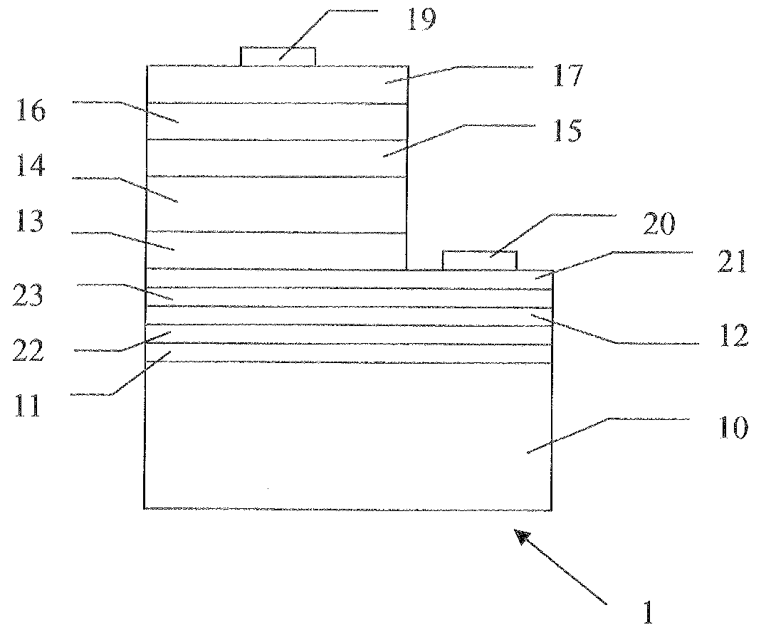
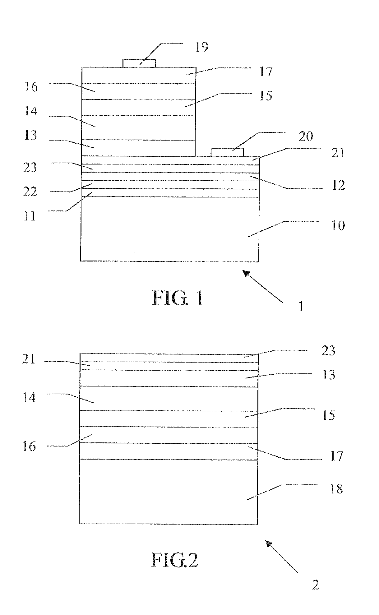
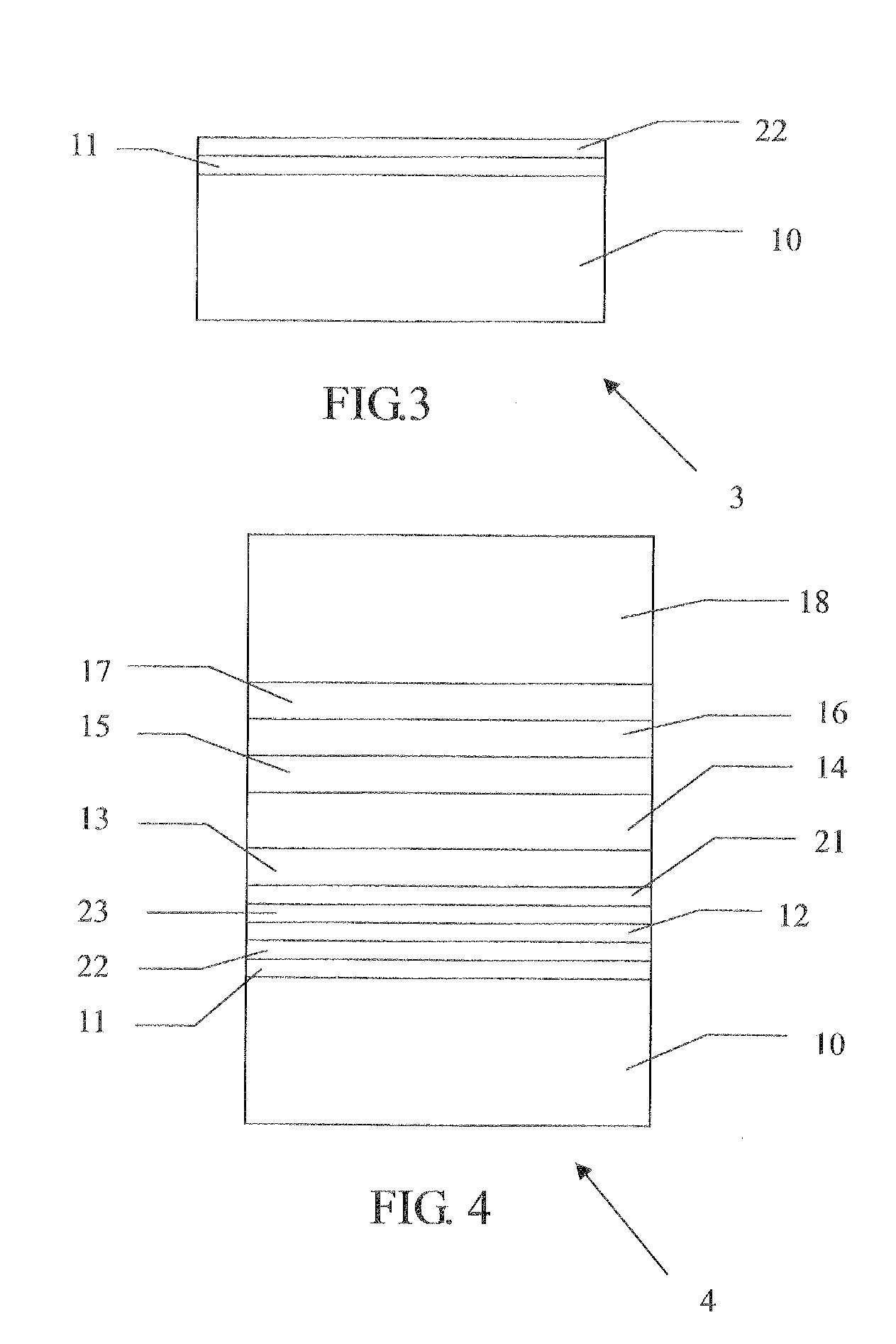
[0027] Referring to FIG. 1, a light emitting diode having an adhesive layer and a reflective layer 1 in accordance with a preferred embodiment of the invention comprises a second substrate 10, a reflective metal layer 11 formed on the second substrate 10, a first reaction layer 22 formed on the reflective metal layer 11, a transparent adhesive layer 12 formed on the first reaction layer 22, a second reaction layer 23 formed on the transparent adhesive layer 12, a transparent conductive layer 21 formed on the second reaction layer 23, wherein the upper surface of the transparent conductive layer 21 consists of a first surface area and a second surface area. A first contact layer 13 is formed on the first surface area. A first cladding layer 14 is formed on the first contact layer 13. An active layer 15 is formed on the first cladding layer 14. A second cladding layer 16 is formed on the active layer 15. A second contact layer 17 is formed on the second cladding layer 16. A first elec...
PUM
 Abstract
Description
Claims
Application Information