Guest-host liquid crystal display panel
- Summary
- Abstract
- Description
- Claims
- Application Information
AI Technical Summary
Benefits of technology
Problems solved by technology
Method used
Image

Examples
first embodiment
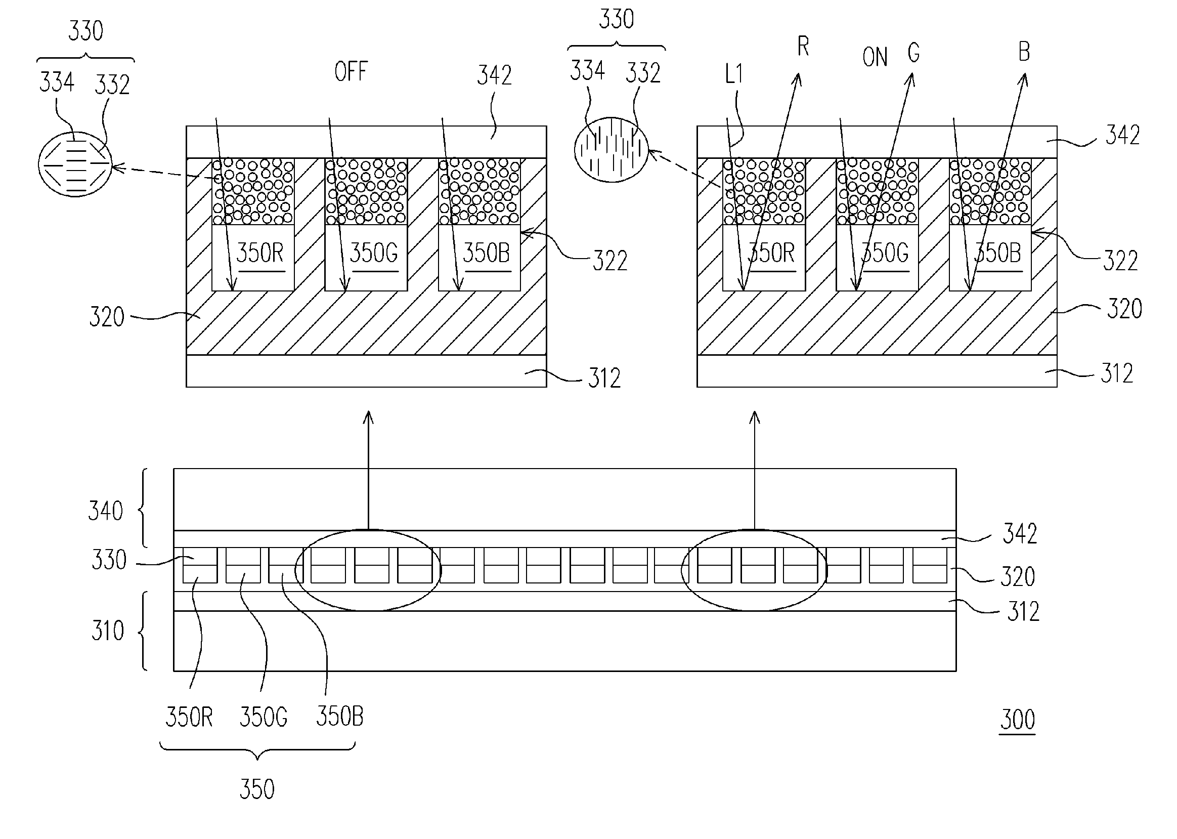
[0025]FIG. 3 is a schematic cross-sectional view of a guest-host LCD panel according to a first embodiment of the present invention. Referring to FIG. 3, the guest-host liquid crystal display panel 300 of the present embodiment comprises a first substrate 310, a display medium accommodating layer 320, a display medium 330, a second substrate 340, and a plurality of color filter layers 350. The first substrate 310 has a first patterned electrode layer 312, and the display medium accommodating layer 320 is disposed on the first patterned electrode layer 312. The display medium accommodating layer 320 has a plurality of micro-cups 322 located above the first patterned electrode layer 312. The display medium 330 is disposed in the micro-cups 322 of the display medium accommodating layer 320, wherein the display medium 330 comprises liquid crystal molecules 332 and dichroic dye molecules 334 dispersed in the liquid crystal molecules 332. Moreover, the second substrate 340 having a second...
second embodiment
[0030]FIG. 4 is a schematic cross-sectional view of a guest-host LCD panel according to a second embodiment of the present invention. Referring to FIG. 4, the guest-host LCD panel 400 of the present embodiment is similar to the guest-host LCD panel 400 of the first embodiment, and the only difference is the location of the color filter layers 350 relative to the display medium 330. In the present embodiment, the color filter layers 350 are disposed above the display medium 330.
third embodiment
[0031]FIG. 5 is a schematic cross-sectional view of a guest-host LCD panel according to a third embodiment of the present invention. Referring to FIG. 5, in the guest-host LCD panel 500 of the present embodiment, the first substrate 310 is an active matrix substrate having an active device 314 (e.g. a TFT) and a pixel electrode 312′. The opposite second substrate 340 has a common electrode 342′. The descriptions of other components are omitted herein.
PUM
| Property | Measurement | Unit |
|---|---|---|
| Dielectric polarization enthalpy | aaaaa | aaaaa |
| Reflection | aaaaa | aaaaa |
Abstract
Description
Claims
Application Information
 - Generate Ideas
- Intellectual Property
- Life Sciences
- Materials
- Tech Scout
- Unparalleled Data Quality
- Higher Quality Content
- 60% Fewer Hallucinations
Browse by: Latest US Patents, China's latest patents, Technical Efficacy Thesaurus, Application Domain, Technology Topic, Popular Technical Reports.
© 2025 PatSnap. All rights reserved.Legal|Privacy policy|Modern Slavery Act Transparency Statement|Sitemap|About US| Contact US: help@patsnap.com