Memory cell comprising switchable semiconductor memory element with trimmable resistance

a memory cell and semiconductor technology, applied in semiconductor devices, digital storage, instruments, etc., can solve the problems of difficult fabrication and operation of three-terminal devices, complex solutions for achieving erasable or multi-state cells, and difficult work of chalcogenides

Active Publication Date: 2007-04-26
WODEN TECH INC
View PDF24 Cites 212 Cited by
  • Summary
  • Abstract
  • Description
  • Claims
  • Application Information

AI Technical Summary

Benefits of technology

[0013] Each of the aspects and embodiments of the invention described herein can be used alone or in combination with one another.
[0014] The preferred aspects and embodiments will now be described with reference to the attached drawings.

Problems solved by technology

Some solutions for achieving erasable or multi-state cells are complex.
These memory cells are three-terminal devices which are relatively difficult to fabricate and operate at the very small dimensions required for competitiveness in modern integrated circuits.
Chalcogenides are difficult to work with and can present challenges in most semiconductor production facilities.

Method used


Image

  • Memory cell comprising switchable semiconductor memory element with trimmable resistance
  • Memory cell comprising switchable semiconductor memory element with trimmable resistance
  • Memory cell comprising switchable semiconductor memory element with trimmable resistance

Examples


Embodiment Construction

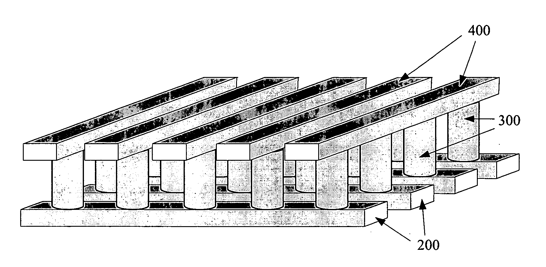
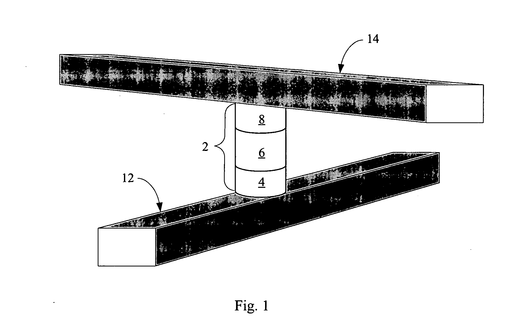
[0007] The present invention is defined by the following claims, and nothing in this section should be taken as a limitation on those claims. In general, the invention is directed to a nonvolatile memory cell having a diode and a semiconductor element with trimmable resistance.

[0008] A first aspect of the invention provides for a method for changing and sensing data states for a nonvolatile memory cell, the method comprising: switching semiconductor material from a first stable resistivity state to a second stable resistivity state, the second resistivity state lower resistivity than the first resistivity state; switching the semiconductor material from the second stable resistivity state to a third stable resistivity state, the third resistivity state higher resistivity than the second resistivity state; and sensing the first resistivity state, the second resistivity state, or the third resistivity state as a data state of the memory cell, wherein the memory cell comprises a porti...


PUM


Abstract

A nonvolatile memory cell comprising doped semiconductor material and a diode can store memory states by changing the resistance of the doped semiconductor material by application of a set pulse (decreasing resistance) or a reset pulse (increasing resistance.) Set pulses are of short duration and above a threshold voltage, while reset pulses are longer duration and below a threshold voltage. In some embodiments multiple resistance states can be achieved, allowing for a multi-state cell, while restoring a prior high-resistance state allows for an rewriteable cell. In some embodiments, the diode and a switchable memory formed of doped semiconductor material are formed in series, while in other embodiments, the diode itself serves as the semiconductor switchable memory element.

Description

BACKGROUND OF THE INVENTION [0001] The invention relates to a nonvolatile memory array. [0002] Nonvolatile memory arrays maintain their data even when power to the device is turned off. In one-time-programmable arrays, each memory cell is formed in an initial unprogrammed state, and can be converted to a programmed state. This change is permanent, and such cells are not erasable. In other types of memories, the memory cells are erasable, and can be rewritten many times. [0003] Cells may also vary in the number of data states, or bits, each cell can achieve. A data state may be stored by altering some characteristic of the cell which can be detected, such as current flowing through the cell under a given applied voltage or the threshold voltage of a transistor within the cell. [0004] Some solutions for achieving erasable or multi-state cells are complex. Floating gate and SONOS memory cells, for example, operate by storing charge, where the presence, absence or amount of stored charg...

Claims


Application Information

Patent Timeline
Patent Type & Authority Applications(United States)
IPC IPC(8): H01L29/94
CPCG11C11/005H01L27/2463G11C11/5692G11C13/0007G11C13/003G11C17/14G11C2211/5641G11C2211/5646G11C2213/32G11C2213/71G11C2213/72G11C2213/76H01L27/101H01L45/08H01L45/1233H01L45/148H01L27/2409G11C11/5685H10B63/20H10B63/80H10N70/24H10N70/884H10N70/826
Inventor KUMAR, TANMAYHERNER, S. BRAD
Owner WODEN TECH INC
Why Eureka
Try Eureka