Biosensor

a biosensor and optical technology, applied in the field of optical biosensors, can solve the problems of large sensor size, high cost, limited vein sensor, etc., and achieve the effect of high light reception efficiency

Inactive Publication Date: 2007-05-03
NEC LCD TECH CORP
View PDF16 Cites 17 Cited by
  • Summary
  • Abstract
  • Description
  • Claims
  • Application Information

AI Technical Summary

Benefits of technology

[0011] An object of the present invention is to provide an optical biosensor that is ca

Problems solved by technology

However, a capacitance fingerprint sensor has the drawback of being susceptible to electrostatic discharge, and since the sensor substrate of an optical fingerprint sensor is a semiconductor, a large sensor is extremely expensive.
Furthermore, vein sensors have also been limited in the past to CCD (Charge Coupled Device) sensors, CMOS (Complementary Metal-Oxide Semiconductor) sensors, and other optical vein sensors.
However, the conventional technique described above has such drawbacks as the follo

Method used


Image

  • Biosensor
  • Biosensor
  • Biosensor

Examples


Embodiment Construction

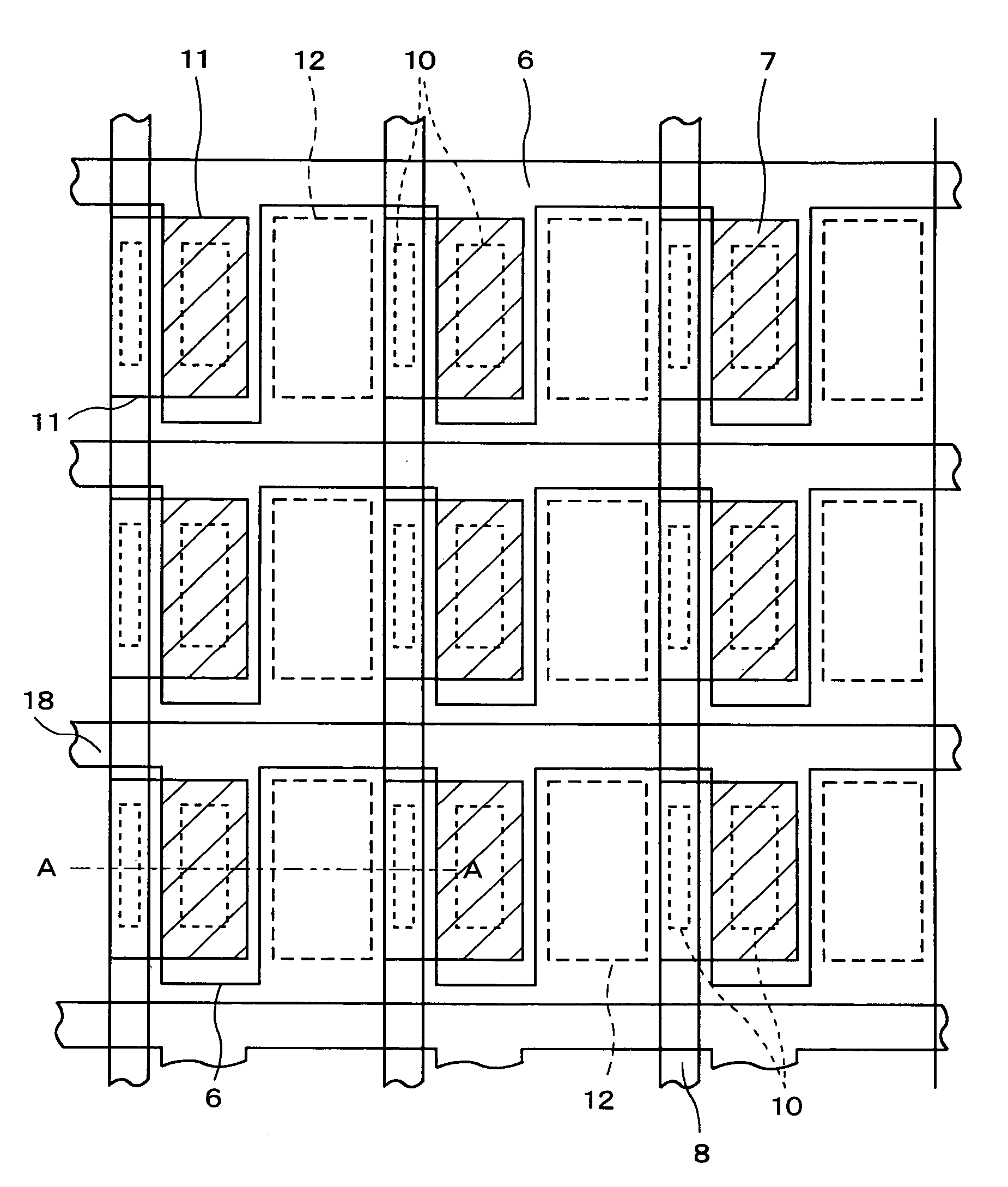
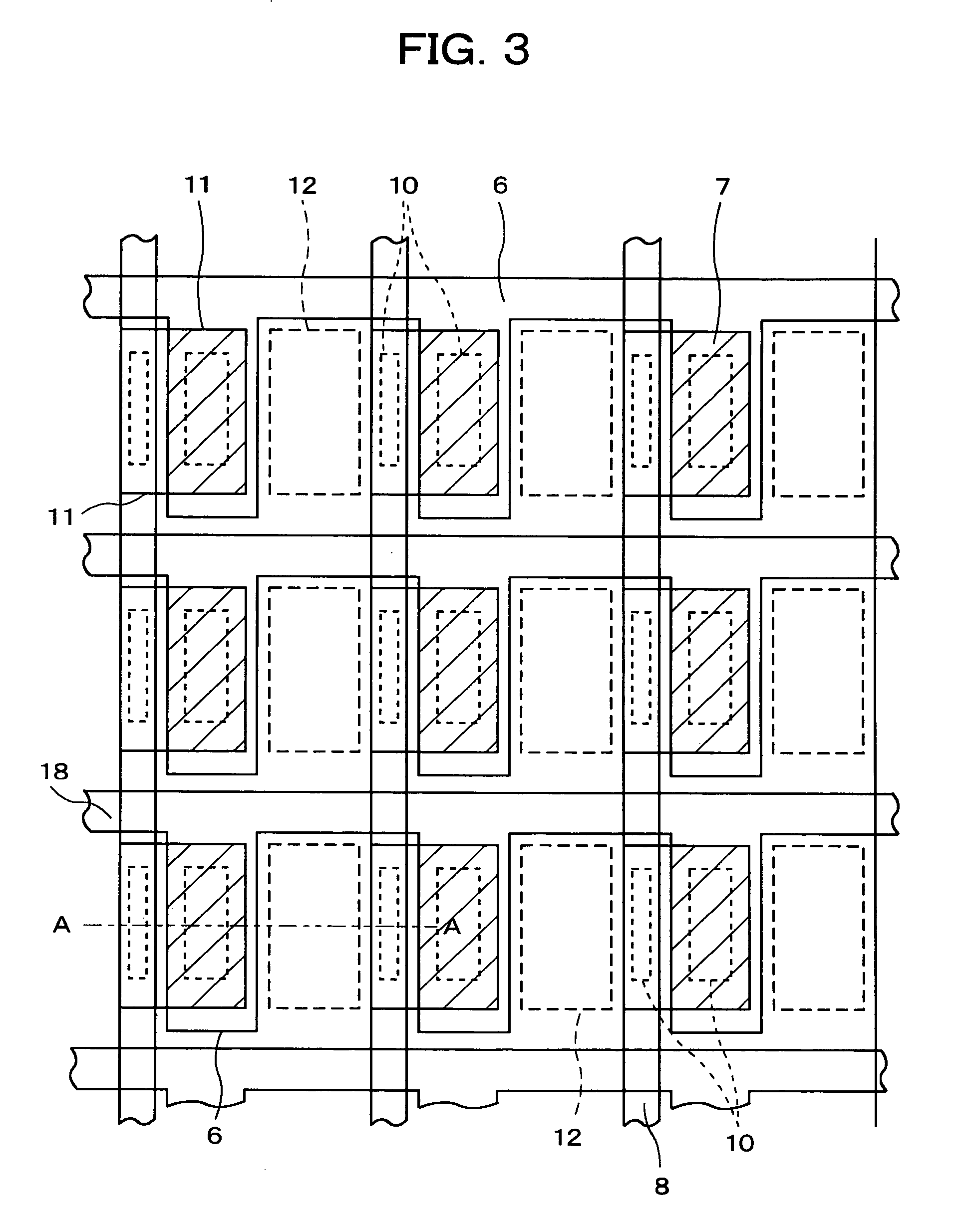
[0025] Embodiments of the present invention will be described in detail hereinafter with reference to the accompanying drawings. FIG. 3 is a plan view showing the unit for detecting a fingerprint or a vein in the biosensor according to the present embodiment, and FIG. 4 is a longitudinal sectional view along line A-A shown in FIG. 3.

[0026] As shown in FIG. 4, a louver 2 is placed on a backlight unit 1 that is composed of an LED (Light Emitting Diode), for example. The louver 2 is a louver film having a thickness of about 300 μm that is composed of a film in which transparent portions and opaque portions are layered in alternating fashion, for example. A light-receiving substrate is also placed on the louver 2. In the light-receiving substrate, a sensor element is formed on a transparent insulating substrate 3 composed of glass, for example. Specifically, an opaque film 4 having an opening 12 is formed on the substrate 3, a transparent insulating film 5 is formed on the opaque film ...


PUM


Abstract

An optical biosensor that is capable of reading a fingerprint or a vein pattern with high efficiency of light reception. A louver is provided between a backlight unit and a substrate in a sensor for identifying a fingerprint by a process in which light emitted from the backlight unit passes through the substrate and is radiated to a fingerprint that is in contact with the upper surface of a protective layer, and light that is reflected according to the surface irregularity of the fingerprint is received by a semiconductor layer that is a light-receiving element. The emitted light is thereby provided with sharp directivity, and the efficiency of light reception by the sensor is therefore increased.

Description

BACKGROUND OF THE INVENTION [0001] 1. Field of the Invention [0002] The present invention relates to an optical biosensor that is capable of reading a fingerprint or a vein pattern. [0003] 2. Description of the Related Art [0004] Biological authentication through identification of fingerprints or vein patterns has recently come into use for ensuring the security of mobile telephones, personal computers, and other devices. A fingerprint sensor may operate optically, or according to capacitance (see Japanese Laid-open Patent Application No. 2002-267408, for example), pressure, or another property, and optical sensors and capacitance sensors are advantageous in terms of precise fingerprint detection. However, a capacitance fingerprint sensor has the drawback of being susceptible to electrostatic discharge, and since the sensor substrate of an optical fingerprint sensor is a semiconductor, a large sensor is extremely expensive. Furthermore, vein sensors have also been limited in the pas...

Claims


Application Information

Patent Timeline
IPC IPC(8): G06K9/00
CPCG06K9/0004G06K2009/00932G06V40/1318G06V40/14
Inventor TAKAHASHI, MITSUASA
Owner NEC LCD TECH CORP
Why Eureka
Try Eureka