Method of forming pattern, film structure, electrooptical device and electronic equipment

a technology of electrooptical devices and patterns, applied in non-linear optics, inspection/indentification of circuits, instruments, etc., can solve the problems of low alignment accuracy, achieve high alignment precision, low transparency, and high recognition accuracy

Inactive Publication Date: 2007-05-03
SEIKO EPSON CORP
View PDF5 Cites 38 Cited by
  • Summary
  • Abstract
  • Description
  • Claims
  • Application Information

AI Technical Summary

Benefits of technology

[0009] An advantage of the present invention is to provide a method of forming a pattern in which a pattern can be formed with a high alignment precision. Another advantage of the present invention is to provide a film structure, an electrooptical device and electronic equipment manufactured by the pattern forming method.
[0010] A method of forming a pattern according to a first aspect of the invention includes forming mark partition walls that correspond to an alignment mark on a substrate before forming the pattern by providing a pattern forming material between partition walls, and providing a liquid material containing an alignment mark forming material between the mark partition walls.
[0011] In the method of forming a pattern according to one aspect o

Problems solved by technology

However, aforementioned technique has the followin

Method used


Image

  • Method of forming pattern, film structure, electrooptical device and electronic equipment
  • Method of forming pattern, film structure, electrooptical device and electronic equipment
  • Method of forming pattern, film structure, electrooptical device and electronic equipment

Examples


Embodiment Construction

[0043] Embodiments of the invention including a method of forming a pattern, a film structure, an electrooptical device and electronic equipment will be described with reference to FIGS. 1 through 14

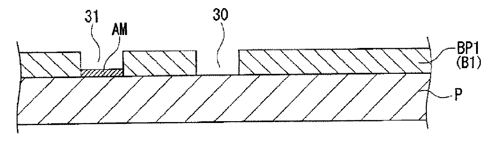
[0044] In the accompanying drawings, a scale size may be different by each member or layer in order to make the member or layer recognizable.

[0045] Electrooptical Device

[0046] An embodiment of an electrooptical device according to the invention is hereinafter described.

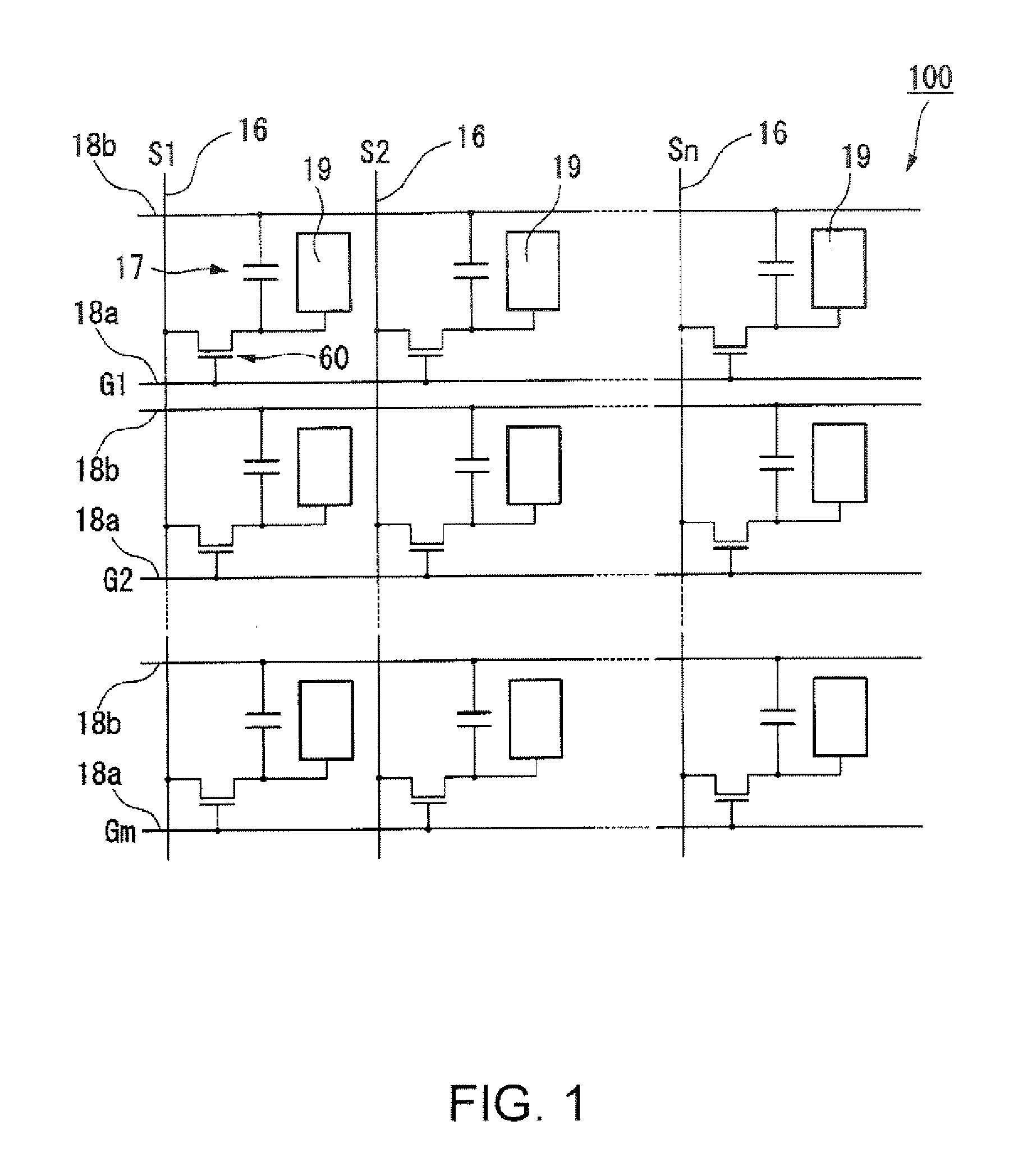
[0047]FIG. 1 is an equivalent circuit diagram of a liquid crystal display device 100 which is an embodiment of the electrooptical device of the invention. A plurality of dots that forms an image display area is arranged in matrix in the liquid crystal display device 100. A pixel electrode 19 and a TFT 60 that is a switching element for controlling the pixel electrode 19 are formed in each dot. A data line (electrode wiring) 16 through which an image signal is supplied is electrically coupled to a source of the TFT 60. I...


PUM


Abstract

A method of forming a pattern includes forming mark partition walls that correspond to an alignment mark on a substrate before forming the pattern by providing a pattern forming material between partition walls, and providing a liquid material containing an alignment mark forming material between the mark partition walls.

Description

BACKGROUND OF THE INVENTION [0001] 1. Technical Field [0002] The present invention relates to a method of forming a pattern, a film structure, an electrooptical device and electronic equipment. [0003] 2. Related Art [0004] A method of forming a conductive pattern by forming a hydrophilic part and a hydrophobic part on a surface of for example a glass substrate and then providing liquid containing metal particles onto the hydrophilic part has been recently developed. JP-A-2002-164635 is an example of related art. According to the example, the hydrophilic part is firstly formed by forming a hydrophobic film which is composed of organic molecules then removing a part of the hydrophobic film (the hydrophobic part). Subsequently, a conductive pattern is formed by filling a discharge head with a liquid that contains metal particles which are the material of the conductive pattern, then discharging the liquid onto the hydrophilic part as relatively moving the discharge head and a substrate...

Claims


Application Information

Patent Timeline
IPC IPC(8): H01L21/00
CPCH01L51/56H05K1/0269H05K3/0008H01L27/1292H05K2201/09918H05K2203/013H05K2203/0568H05K3/125H10K71/00G02F1/1339
Inventor HIRAI, TOSHIMITSUMORIYA, KATSUYUKIINAGAKI, AKIRA
Owner SEIKO EPSON CORP
Why Eureka
Try Eureka