Stack-type semiconductor device and method of manufacturing the same
a semiconductor device and stack-type technology, applied in the direction of electrical apparatus construction details, casings/cabinets/drawers, casings/cabinets/drawers details, etc., can solve the problems of inability to enhance the reliability of stack-type memory devices, the wires for connecting the top layer semiconductor chip electrode and the lead frame are inevitably too long, and the bonding design becomes difficul
- Summary
- Abstract
- Description
- Claims
- Application Information
AI Technical Summary
Problems solved by technology
Method used
Image

Examples
first embodiment
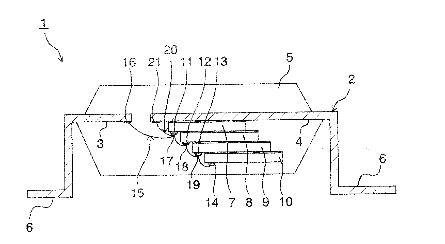
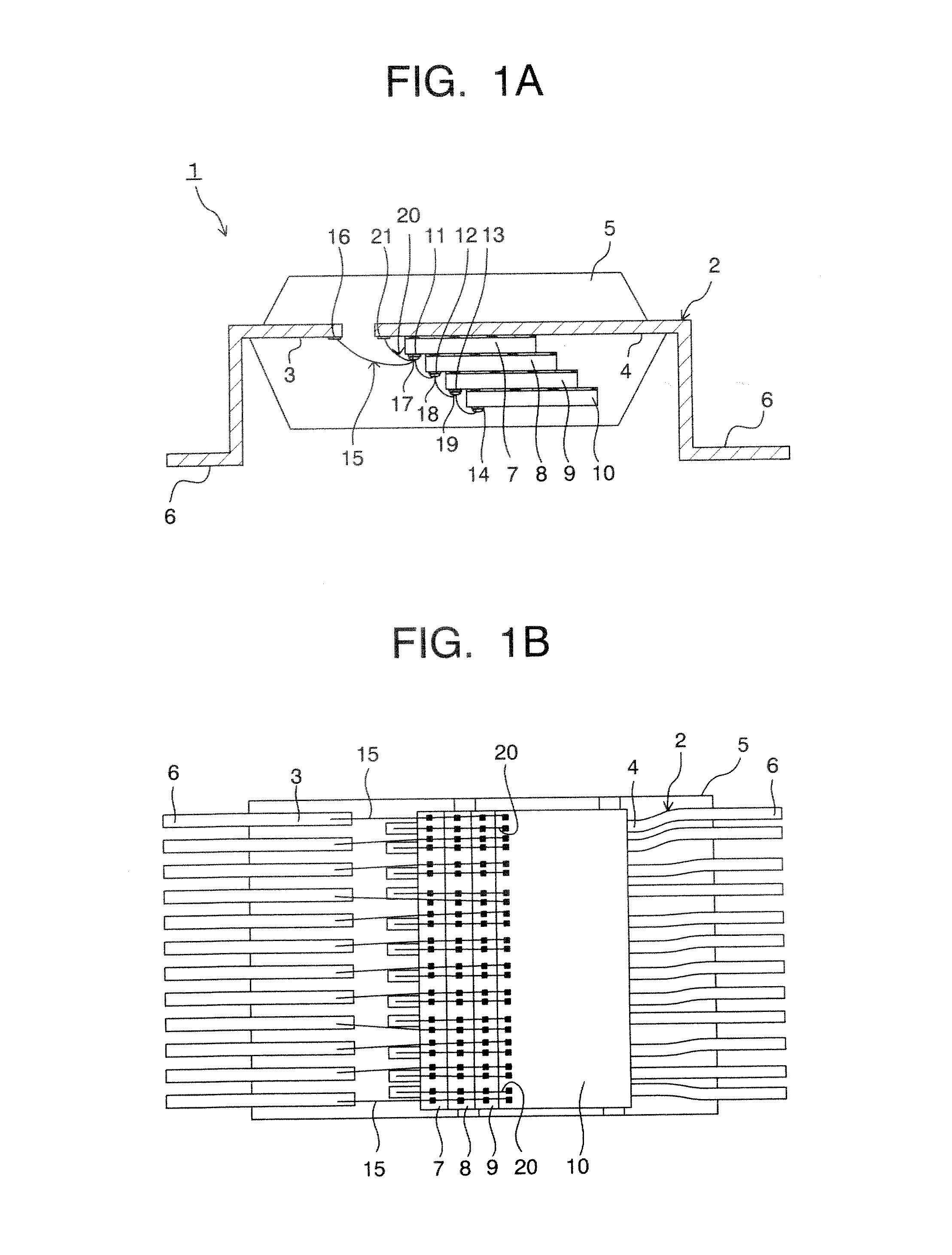
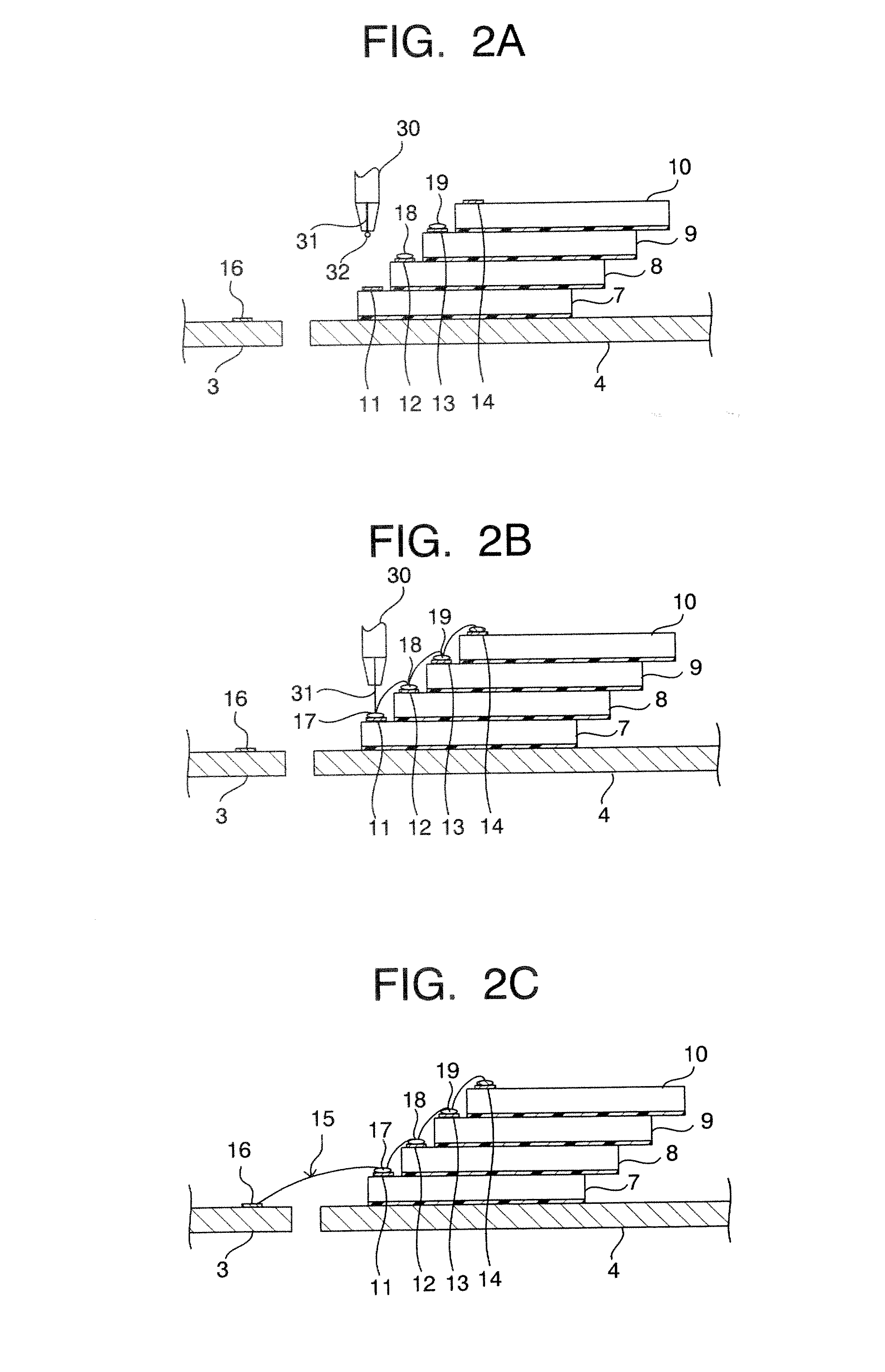
[0023]FIG. 1A is a cross-sectional view schematically showing the structure of a stack-type semiconductor device according to the present invention, and FIG. 1B is a plan view of the structure of the stack-type semiconductor device as shown in FIG. 1A, as viewed from the backside of the semiconductor device under the state without a sealing resin. In this embodiment, the stack-type semiconductor device 1 is directed at a TSOP (Thin Small Outline Package) structured semiconductor device in which four semiconductor chips are stacked and packaged under the face-down condition. The stack-type semiconductor device 1 shown in FIGS. 1 includes a lead frame 2 as a circuit board. Instead of the lead frame, another circuit board may be employed.
[0024] The lead frame 2 includes first inner leads 3 and second inner leads 4 which have the respective different lengths, and outer leads 6 which are continued from the inner leads 3 and 4 through a sealing resin 5. The inner leads 3 and 4 are not dep...
second embodiment
[0054] The lead frame is not limited to the embodiment relating to FIG. 6 and may be constructed from the one as shown in FIG. 7FIG. 7 is a plan view showing another lead frame to be employed in the stack-type semiconductor device according to the present invention. The external terminals VCC, VSS, I / O-0˜I / 0-7, RB, CE, RE, CLE, ALE, WE, WP are allotted in the same manner as the electrode pads 61 of the NAND-type flash memory 60. Herein, the reference numeral “N.C” designates the condition of nonuse. A lead frame 2B is illustrated in which the first inner leads 3 and the second inner leads 4 are divided into two sections, respectively so that the forefronts of the first inner leads 3 are arranged outside the forefronts of the second inner leads 4.
[0055] According to this embodiment, therefore, since the first bonding wires 15 and the second bonding wires 20 are wire-bonded to the fourth electrode pads 14 and the bonding pads 16,21 of the first inner leads 3 and the second inner leads...
PUM
 Abstract
Description
Claims
Application Information
 - Generate Ideas
- Intellectual Property
- Life Sciences
- Materials
- Tech Scout
- Unparalleled Data Quality
- Higher Quality Content
- 60% Fewer Hallucinations
Browse by: Latest US Patents, China's latest patents, Technical Efficacy Thesaurus, Application Domain, Technology Topic, Popular Technical Reports.
© 2025 PatSnap. All rights reserved.Legal|Privacy policy|Modern Slavery Act Transparency Statement|Sitemap|About US| Contact US: help@patsnap.com