Method of managing fails in a non-volatile memory device and relative memory device

a non-volatile memory device and relative memory technology, applied in the field of memory devices, can solve the problems of high voltage damage to the cells, block damage, and intrinsic efficiency problems of the nand flash memory device, and achieve the effect of low cost integration and easy implementation

Active Publication Date: 2007-05-17
MICRON TECH INC
View PDF11 Cites 451 Cited by
  • Summary
  • Abstract
  • Description
  • Claims
  • Application Information

AI Technical Summary

Benefits of technology

[0017] An object of the invention is to provide a method of managing fails in a non-volatile memory device

Problems solved by technology

NAND FLASH memory devices have intrinsic problems of efficiency due to the peculiar architecture of the array of cells, and to the relatively high voltages that are applied during program operations.
The high voltages may damage the cells.
If the spare area associated to a block does not store the code FFh in the first page, it then means that the block has been marked bad.
During the working life of the memory device, in any case after the EWS phase, some blocks initially recognized as good may become unusable because one or more cells of the block fails.
Newly developed bad bl

Method used


Image

  • Method of managing fails in a non-volatile memory device and relative memory device
  • Method of managing fails in a non-volatile memory device and relative memory device
  • Method of managing fails in a non-volatile memory device and relative memory device

Examples


Embodiment Construction

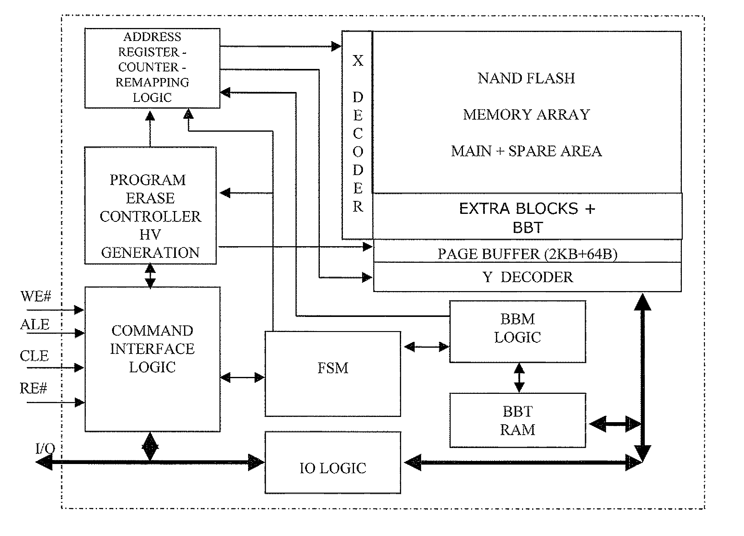
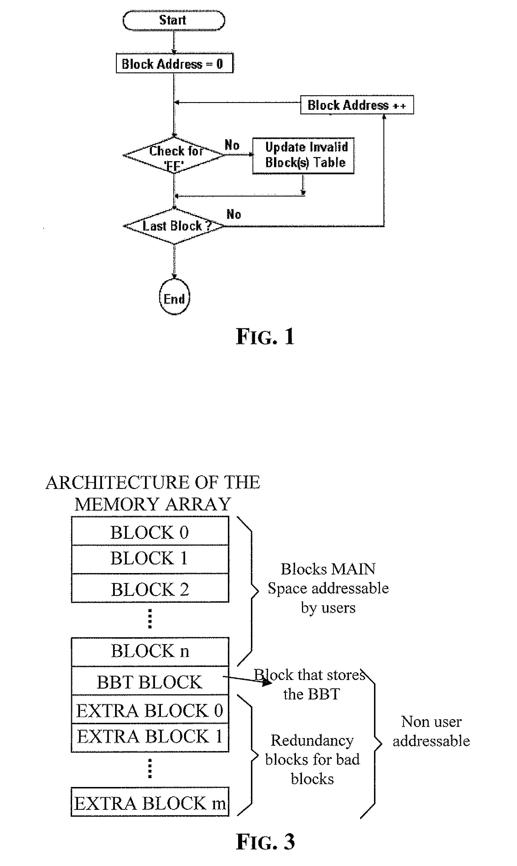
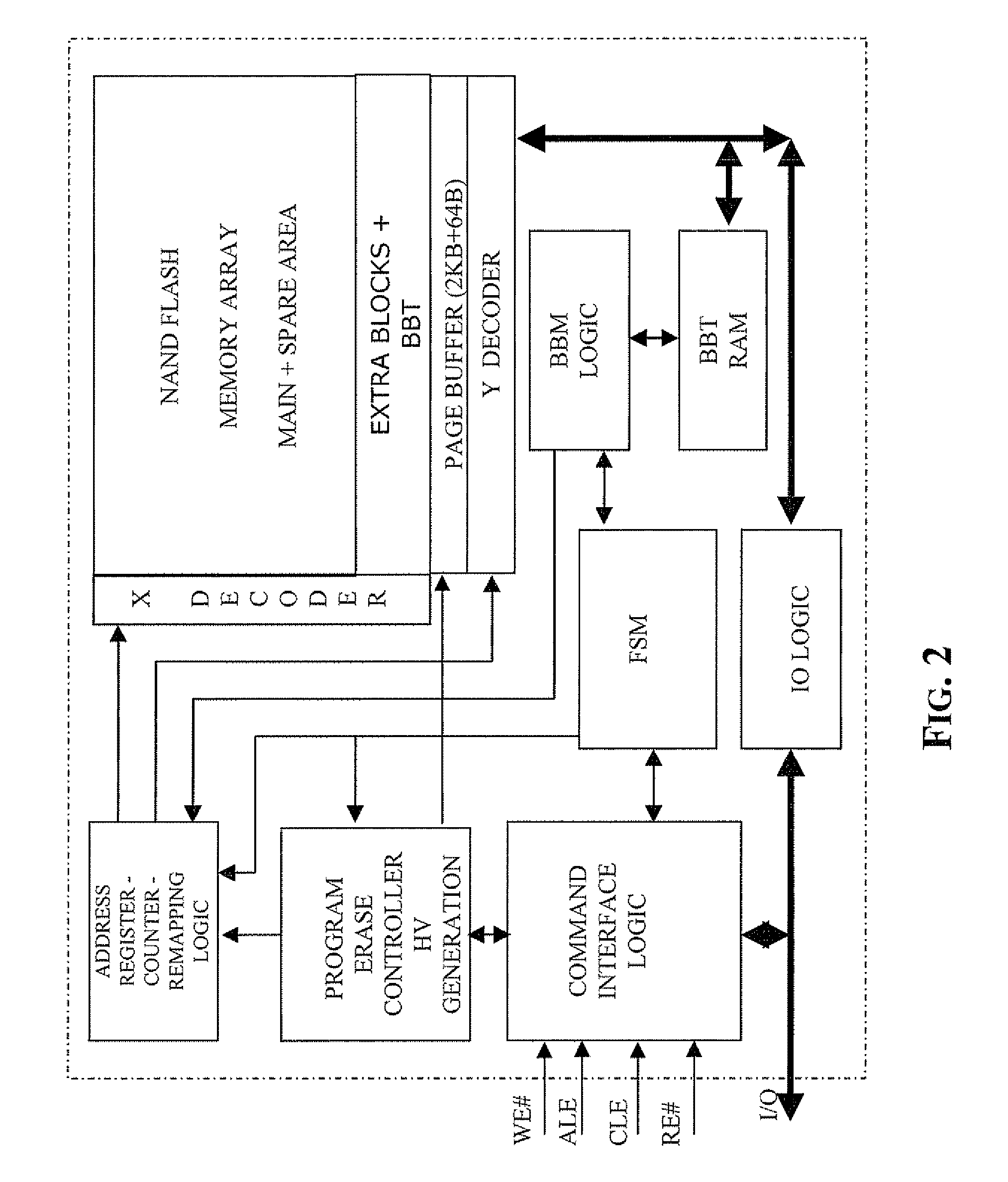
[0035] A basic architecture of a memory device that implements the method of the invention is depicted in FIG. 2. The array of memory cells is divided into first, second and third subsets. The first subset (MAIN) is composed of user addressable blocks of cells. The second subset (EXTRA BLOCKS) is composed of blocks of redundancy cells. The third subset (BBT) is for storing the table of addresses of bad blocks.

[0036] A fourth subset SPARE AREA of dedicated cells for storing the code (FFh) in a first page of each block acknowledged as good could still be present as a reserved tool for checking the statues, but it is not necessary for the management of fails according to the invention.

[0037] The meaning of the other functional blocks depicted in FIG. 2 is clarified in TABLE 1:

TABLE 1ADDRESSRegister that stores the address of theREGISTERcurrently addressed page.COUNTERAddress counter of the array, used duringalgorithms for accessing the array (read,program, erase).REMAPPINGLogic cir...


PUM


Abstract

A method of managing fails in a non-volatile memory device including an array of cells grouped in blocks of data storage cells includes defining in the array a first subset of user addressable blocks of cells, and a second subset of redundancy blocks of cells. Each block including at least one failed cell in the first subset is located during a test on wafer of the non-volatile memory device. Each block is marked as bad, and a bad block address table of respective codes is stored in a non-volatile memory buffer. At power-on, the bad block address table is copied from the non-volatile memory buffer to the random access memory. A block of memory cells of the first subset is verified as bad by looking up the bad block address table, and if a block is bad, then remapping access to a corresponding block of redundancy cells. A third subset of non-user addressable blocks of cells is defined in the array for storing the bad block address table of respective codes in an addressable page of cells of a block of the third subset. Each page of the third subset is associated to a corresponding redundancy block. If during the working life of the memory device a block of cells previously judged good in a test phase becomes failed, each block is marked as bad and the stored table in the random access memory is updated.

Description

FIELD OF THE INVENTION [0001] The invention relates to memory devices, and more particularly, to a method of managing failed blocks of array cells and to a non-volatile memory device comprising dedicated logic circuits for implementing the method. BACKGROUND OF THE INVENTION [0002] NAND FLASH memories are large integration scale devices capable of storing vast amounts of data. These devices have a cell array organized in blocks of memory cells electrically connected in series. Each block is generally organized in a certain number of pages of data storage space. Because of their commercial importance, reference will be made to these FLASH memory devices, but the technical approaches that will be described may be implementable in any non-volatile memory of similar architecture and constraints. [0003] NAND FLASH memory devices have intrinsic problems of efficiency due to the peculiar architecture of the array of cells, and to the relatively high voltages that are applied during program...

Claims


Application Information

Patent Timeline
IPC IPC(8): G11C16/06
CPCG11C29/006G11C29/76G11C2029/1208
Inventor PELLICONE, DEMETRIOCORSI, ADAMOROVEDA, MARCODI TUORO, CONCETTACARANNANTE, PROCOLOFERRANTE, GIANFRANCO
Owner MICRON TECH INC
Why Eureka
Try Eureka