Thermally developable materials with backside conductive layer

a technology of backside conductive layer and thermo-developable materials, which is applied in the field of thermo-developable materials, can solve the problems of increasing the formation of various types of “fog” or other undesirable sensitometric side effects, distinctly different problems, and much effort in the preparation and manufacture of photo-thermographic materials, so as to improve the conductive efficiency and conductivity. exceptional, the effect of reducing the overall dry thickness of such layers

Inactive Publication Date: 2007-05-17
CARESTREAM HEALTH INC
View PDF24 Cites 0 Cited by
  • Summary
  • Abstract
  • Description
  • Claims
  • Application Information

AI Technical Summary

Benefits of technology

[0052] The present invention provides a means for providing exceptional conductivity on a backside conductive layer with the use of a unique amount of conductive metal antimonate in the backside conductive layer to provide improved conductive efficiency. It was surprising that a lesser amount of conductive metal antimonate particles could be used to provide the same or improved conductivity especially in “buried” conductive layers. The overall dry thickness of such layers can also be reduced because it has been discovered that a lesser amount of binder polymer(s) is needed to achieve the desired layer integrity and adhesion to other layers or to the support. In some embodiments, the improved conductive layer is the only backside layer in the thermally developable materials but in preferred embodiments, the conductive layer is “buried” and the binders of that layer and the overlying conductive layer are designed for maximum adhesion and coating advantages. It has also been found that formulations containing high amounts of non-acicular zinc antimonate (that is, a low binder to non-acicular zinc antimonate ratio) provide highly conductive materials having decreased loss of resistivity when scaled-up under high shear conditions.

Problems solved by technology

The incorporation of the developer into photothermographic materials can lead to increased formation of various types of “fog” or other undesirable sensitometric side effects.
Therefore, much effort has gone into the preparation and manufacture of photothermographic materials to minimize these problems.
Moreover, in photothermographic materials, the unexposed silver halide generally remains intact after development and the material must be stabilized against further imaging and development.
Because photothermographic materials require dry thermal processing, they present distinctly different problems and require different materials in manufacture and use, compared to conventional, wet-processed silver halide photographic materials.
The incorporation of such additives as, for example, stabilizers, antifoggants, speed enhancers, supersensitizers, and spectral and chemical sensitizers in conventional photographic materials is not predictive of whether such additives will prove beneficial or detrimental in photothermographic materials.
The accumulated charges can cause various problems.
This may result in imaging defects that are a particular problem where the images are used for medical diagnosis.
Build-up of electrostatic charge can also cause sheets of thermally processable materials to stick together causing misfeeds and jamming within processing equipment.
Additionally, accumulated electrostatic charge can attract dust or other particulate matter to the materials, thereby requiring more cleaning to insure rapid transport through the processing equipment and quality imaging.
Build-up of electrostatic charge also makes handling of developed sheets of imaged material more difficult.
This problem can be particularly severe when reviewing an imaged film that has been stored for a long period of time because many antistatic materials loose their effectiveness over time.
Despite these advances, little attention has been paid to the effect of large-scale processing conditions on the “conductive efficiency” of the formulations described above.
For example, when production quantities of backside conductive materials are prepared, the speed required for efficient mixing often results in shear conditions that are different from those involved for the preparation of laboratory quantities.
Often these different properties result in materials having poorer conductive efficiency.

Method used


Image

  • Thermally developable materials with backside conductive layer
  • Thermally developable materials with backside conductive layer
  • Thermally developable materials with backside conductive layer

Examples


example 1

Photothermographic Materials with Improved Conductive Efficiency

[0263] Photothermographic materials were prepared containing buried backside antistatic layers. The ratio of non-acicular zinc antimonate [CELNAX® CX-Z 641M (ZnSb2O6)] to binder was varied. A control sample was also prepared containing a ratio of binder to non-acicular zinc antimonate as described in U.S. Pat. No. 6,689,546 (noted above).

[0264] Buried Backside Conductive Layer Formulation:

[0265] A buried backside conductive layer formulation was prepared by mixing the following materials:

Solution A:VITEL ® PE-2700B LMW(see TABLE I below)CAB 381-20(see TABLE I below)MEK1,269 g

[0266]

Solution B:CELNAX ® CX-Z641M(see TABLE I below)(containing 60% non-acicular zinc antimonatesolids in methanol)MEK120 g

[0267] Solution A: VITEL® PE-2700B LMW and CAB 381-20 were dissolved in 1.269 Kg of MEK.

[0268] Solution B: CELNAX® CX-Z641M non-acicular zinc antimonate was placed in a second reaction vessel, stirring was begun and 120 g...

example 2

Effect Of Binder to CELNAX® Non-Acicular Zinc Antimonate Ratio on Adhesion to the Support

[0286] The following Example demonstrates the effect of the binder to CELNAX® non-acicular zinc antimonate ratio on adhesion of the backside conductive layer and backside topcoat layer to the support.

[0287] Buried Backside Conductive Layer Formulation:

[0288] A buried backside conductive layer formulation was prepared by mixing the following materials:

CELNAX ® CX-Z641M(see TABLE III below)(containing 60% non-acicular zinc antimonatesolids in methanol)MEK(see TABLE III below)VITEL ® PE-2700B LMW(see TABLE III below)CAB 381-20(see TABLE III below)

[0289] Backside Topcoat Formulation:

[0290] A backside topcoat formulation was prepared by mixing the following materials:

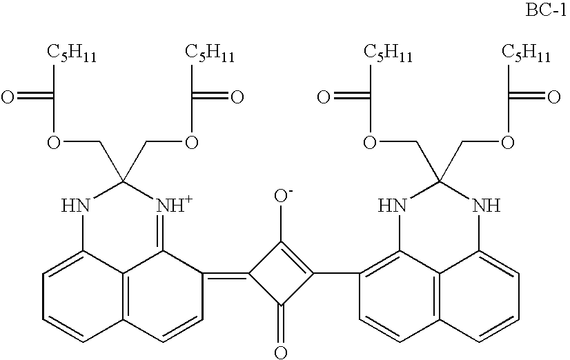
MEK88.9 weight %CAB 381-2010.7 weight %SYLOID ® 74X60000.28 weight %Antihalation Dye BC-10.14 weight %

[0291] The buried backside conductive layer formulation and backside topcoat formulations were simultaneously coated onto one s...

example 3

Effect of Mixing Shear on Resistivity

[0294] When production quantities of materials are prepared, the speed required for efficient mixing often results in shear conditions that are different from those involved for the preparation of laboratory quantities. As a result, the materials so produced can have properties different from those of laboratory-prepared samples. The following example demonstrates the effect of high shear mixing on the resistivity of the resulting backside layer.

[0295] Conductive backside coating formulations were prepared as described in Example 2 containing various ratios of binder to non-acicular zinc antimonate [CELNAX®, (ZnSb2O6)].

[0296] Formulations were coated before and after being subjected to high shear homogenization. Homogenization was carried for one pass at 8,000 psi using a Model 15 MR Laboratory Homogenizer manufactured by APV Gaulin, Inc. (Everett, Mass.). A control sample was also prepared containing a ratio of binder to non-acicular zinc ant...


PUM

PropertyMeasurementUnit
thicknessaaaaaaaaaa
thicknessaaaaaaaaaa
thicknessaaaaaaaaaa

Abstract

Thermally developable materials that comprise a support have a conductive backside layer that has increased conductive efficiency. Conductivity is provided by non-acicular metal antimonate particles that are present in an amount greater than 55 and up to 85 dry weight % at a coverage of from about 0.06 to about 0.5 g / m2, and the ratio of total binder polymers in the backside conductive layer to the non-acicular metal antimonate particles is less than 0.75:1 (dry weights). The level of conductive particles is reduced from previous uses without an unacceptable loss in conductivity. In addition, the dry thickness of the conductive layer is considerably reduced.

Description

FIELD OF THE INVENTION [0001] This invention relates to thermally developable materials having certain backside conductive layers. In particular, this invention relates to thermographic and photothermographic materials having conductive backside layers with improved “conductive efficiency.” This invention also relates to methods of imaging using these thermally developable materials. BACKGROUND OF THE INVENTION [0002] Silver-containing thermographic and photothermographic imaging materials (that is, thermally developable imaging materials) that are imaged and / or developed using heat and without liquid processing have been known in the art for many years. [0003] Silver-containing thermographic imaging materials are non-photo-sensitive materials that are used in a recording process wherein images are generated by the use of thermal energy. These materials generally comprise a support having disposed thereon (a) a relatively or completely non-photosensitive source of reducible silver i...

Claims


Application Information

Patent Timeline
Patent Type & Authority Applications(United States)
IPC IPC(8): G03C1/00
CPCG03C1/49818G03C1/49872G03C1/853G03C2001/03541G03C1/0051G03C1/825G03C1/85G03C2001/7628G03C2200/47
Inventor LUDEMANN, THOMAS J.LABELLE, GARY E.KOESTNER, ROLAND J.HEFLEY, JOHN P.BHAVE, APARNA V.GEISLER, THOMAS C.PHILIP, DARLENE F.
Owner CARESTREAM HEALTH INC
Why Eureka
Try Eureka