Low power testing of very large circuits

a very large circuit and low power technology, applied in the direction of electronic circuit testing, measurement devices, instruments, etc., can solve the problems of circuits consuming a significant amount of power and the speed at which these circuits opera

Inactive Publication Date: 2007-05-17
TEXAS INSTR INC
View PDF6 Cites 0 Cited by
  • Summary
  • Abstract
  • Description
  • Claims
  • Application Information

AI Technical Summary

Benefits of technology

[0008] The present invention provides a method of reducing the test operation power by improving upon the scan test methodology such that only portions of the scan circuitry are activated at any one time. By activating only portions of the overall scan circuitry, the power consumed during scan testing can be significantly reduced, especially in ICs designed with CMCS technology. Advantageously, the present invention achieves this lower power scan mode without increasing test time over the conventional scan test methodology. The improvements brought forth by the present invention can be applied in both single scan path test methodologies and in parallel scan path test methodologies. While the following description will teach the improvement as being incorporated in an IC, the improvement can be used at any level of circuit implementation. For example, intellectual property (IP) cores, which are predesigned subcircuits used to design highly complex system ICs, may themselves incorporate the improvement to lower their power consumption during test inside the system IC.

Problems solved by technology

Also, the speed at which these circuits operate increases.
Dynamically activating the combinational logic during scan operations can cause the circuit to consume a significant amount of power.

Method used


Image

  • Low power testing of very large circuits
  • Low power testing of very large circuits
  • Low power testing of very large circuits

Examples


Embodiment Construction

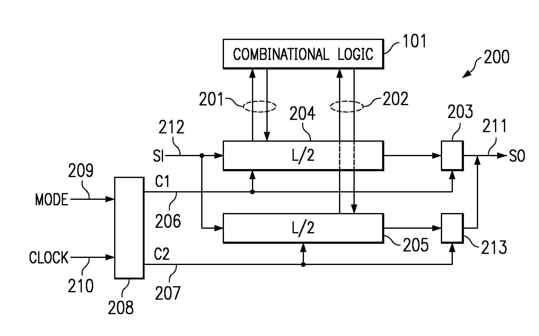
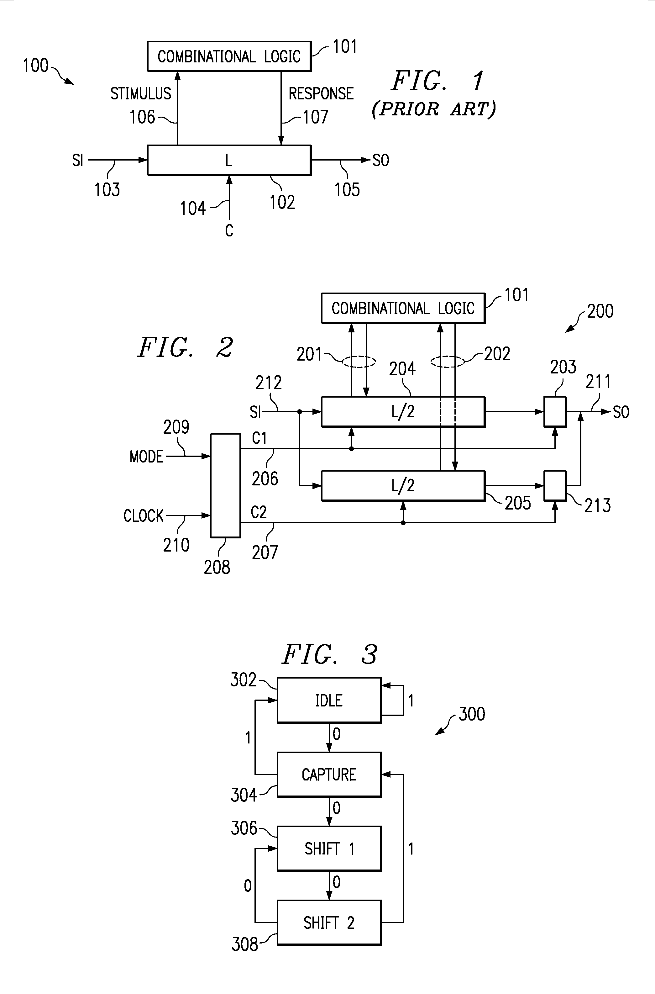
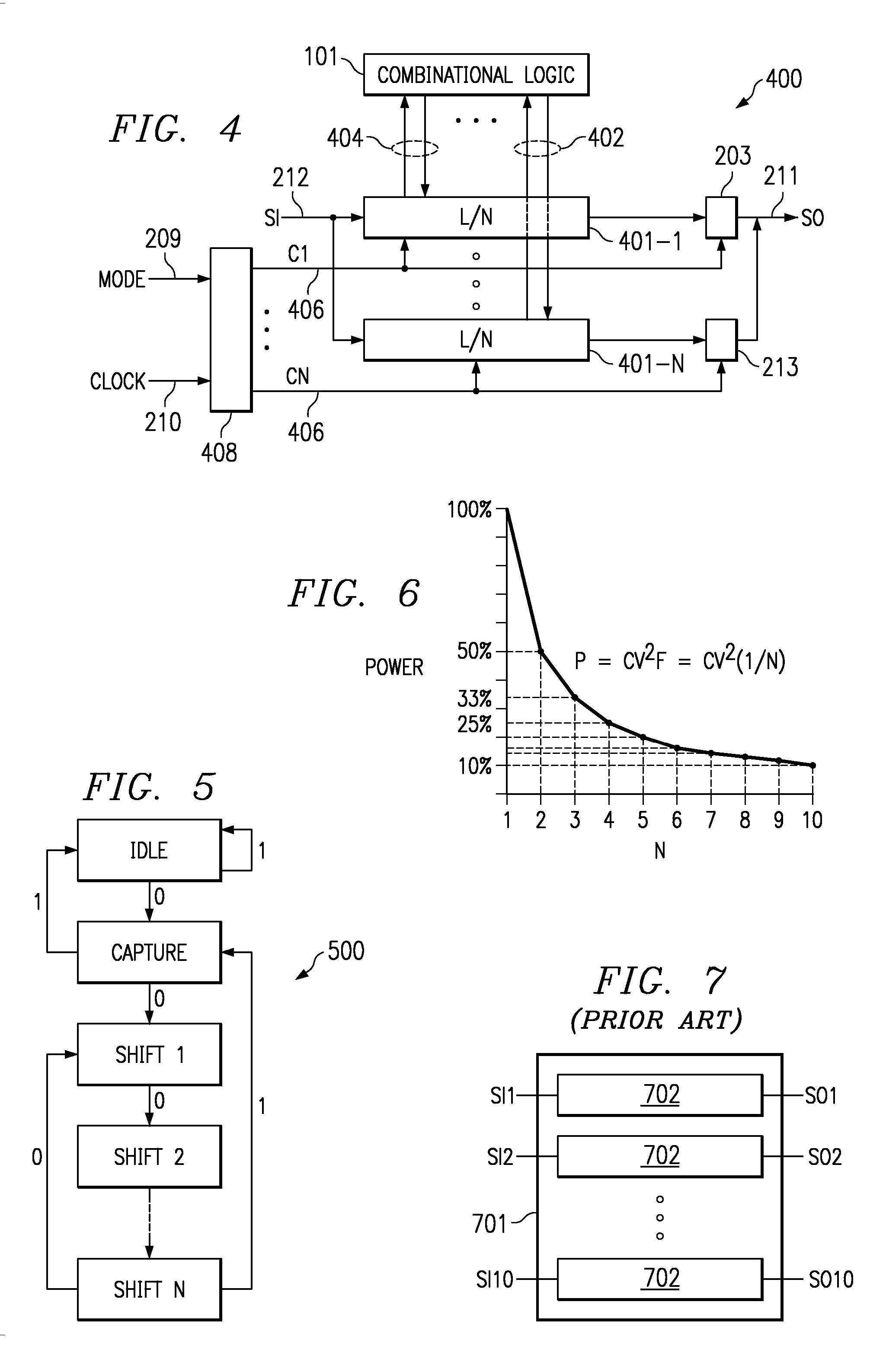
[0016] In FIG. 1 a circuit 100 is placed in a conventional scan test mode. The circuit 100 could be an IC or die, or a subcircuit (core) within an IC or die. In functional mode, the circuit could be a microprocessor, DSP, serial I / O peripheral, or other circuit function. The model illustrates that, during scan test mode, the circuit is partitioned into combinational logic 101 and scan path 102. Scan path 102 comprises functional registers of the circuit (latches / DFFs) 101 that are converted, during test mode, into serially connected scan cells.

[0017] The number of serially connected scan cells determines the length (L) of scan path 102. Each scan cell provides a stimulus input to and response output from combinational logic 101 using interconnects 106 and 107, respectively. The interconnects 106 and 107 are the same interconnects used by the functional registers to communicate functional input and output to the combinational logic during functional mode of the circuit. Scan path 10...


PUM


Abstract

Plural scan test paths (401) are provided to reduce power consumed during testing such as combinational logic (101). A state machine (408) operates according to plural shift states (500) to control each scan path in capturing data from response outputs of the combinational logic and then shifting one bit at a time to reduce the capacitive and constant state power consumed by shifting the scan paths.

Description

[0001] This application is a divisional of application Ser. No. 10 / 771,768, filed Feb. 2, 2004, currently pending; [0002] Which was a divisional of application Ser. No. 10 / 336,985, filed Jan. 6, 2003, now U.S. Pat. No. 6,694,467, issued Feb. 17, 2004; [0003] Which was a divisional of application Ser. No. 09 / 339,734, filed Jun. 24, 1999, now U.S. Pat. No. 6,519,729, issued Feb. 11, 2003; [0004] Which claimed priority from Provisional Application No. 60 / 090,935, filed Jun. 27, 1998.FIELD OF THE INVENTION [0005] This invention relates generally to reducing the power needed to test very large integrated and other circuits with serial and parallel scan paths and in particular relates to reducing the power required to perform these tests by dividing the scan paths into shorter scan paths and shifting each shorter scan path separately. BACKGROUND [0006] As transistor and interconnect geometry's shrink, the number of transistors capable of being connected together to form circuits in an int...

Claims


Application Information

Patent Timeline
Patent Type & Authority Applications(United States)
IPC IPC(8): G01R31/28G01R31/317G01R31/3185
CPCG01R31/31721G01R31/3177G01R31/318575G01R31/318555
Inventor WHETSEL, LEE D.
Owner TEXAS INSTR INC
Why Eureka
Try Eureka