Planar light source and method for fabricating the same

a technology of planar light source and fabricating method, which is applied in the manufacture of electrode systems, electric discharge tubes/lamps, instruments, etc., can solve the problems of uneven thickness of pattern films, uneven emission performance of different areas, and complicated fabrication process of conventional planar light source, so as to prevent cracks in the substrate and increase the coating area of phosphor layers

Inactive Publication Date: 2007-05-24
CHUNGHWA PICTURE TUBES LTD
View PDF12 Cites 4 Cited by
  • Summary
  • Abstract
  • Description
  • Claims
  • Application Information

AI Technical Summary

Benefits of technology

[0011] Accordingly, the present invention is directed to provide a planar light source which can increase the coating area of the phosphor layer and prevent cracks in the substrate.
[0012] According to another aspect of the present invention, a fabricating method for a planar light source is provided, which has simple process and can increase the yield of the planar light source.
[0029] Since in the present invention, dielectric spacers are used to replace the conventional spacers, the space occupied by the conventional spacers can be reduced and the discharge space of the planar light source in the present invention can be increased. Accordingly, the coating area of the phosphor layer in the discharge spaces can be increased. Moreover, the dielectric spacers are formed through a photolithography process. Because of without using frit glue, cracks can be prevented in the substrate. Furthermore, because the dielectric spacers are formed in a film deposition process combined with a photolithography process, the fabricating process of the planar light source in the present invention is simpler compared to the conventional process of fabricating the dielectric layer by multiple printing processes. Accordingly, the yield of planar light source can be increased.

Problems solved by technology

Moreover, the fabricating process of the conventional planar light source is very complicated. FIG. 2 is the fabricating flowchart of a lower substrate of the planar light source in FIG. 1.
Moreover, the printing process may result in uneven thickness of the pattern film due to printing shift; accordingly the light-emitting performance of different areas may be very different.
Since a plurality of spacers 170 are pasted respectively on the lower substrate 120 by the frit glue 190, the process of disposing the spacers 170 will be time-consuming and complicated, thus the production capacity of the planar light source 100 cannot be improved.

Method used


Image

  • Planar light source and method for fabricating the same
  • Planar light source and method for fabricating the same
  • Planar light source and method for fabricating the same

Examples


Embodiment Construction

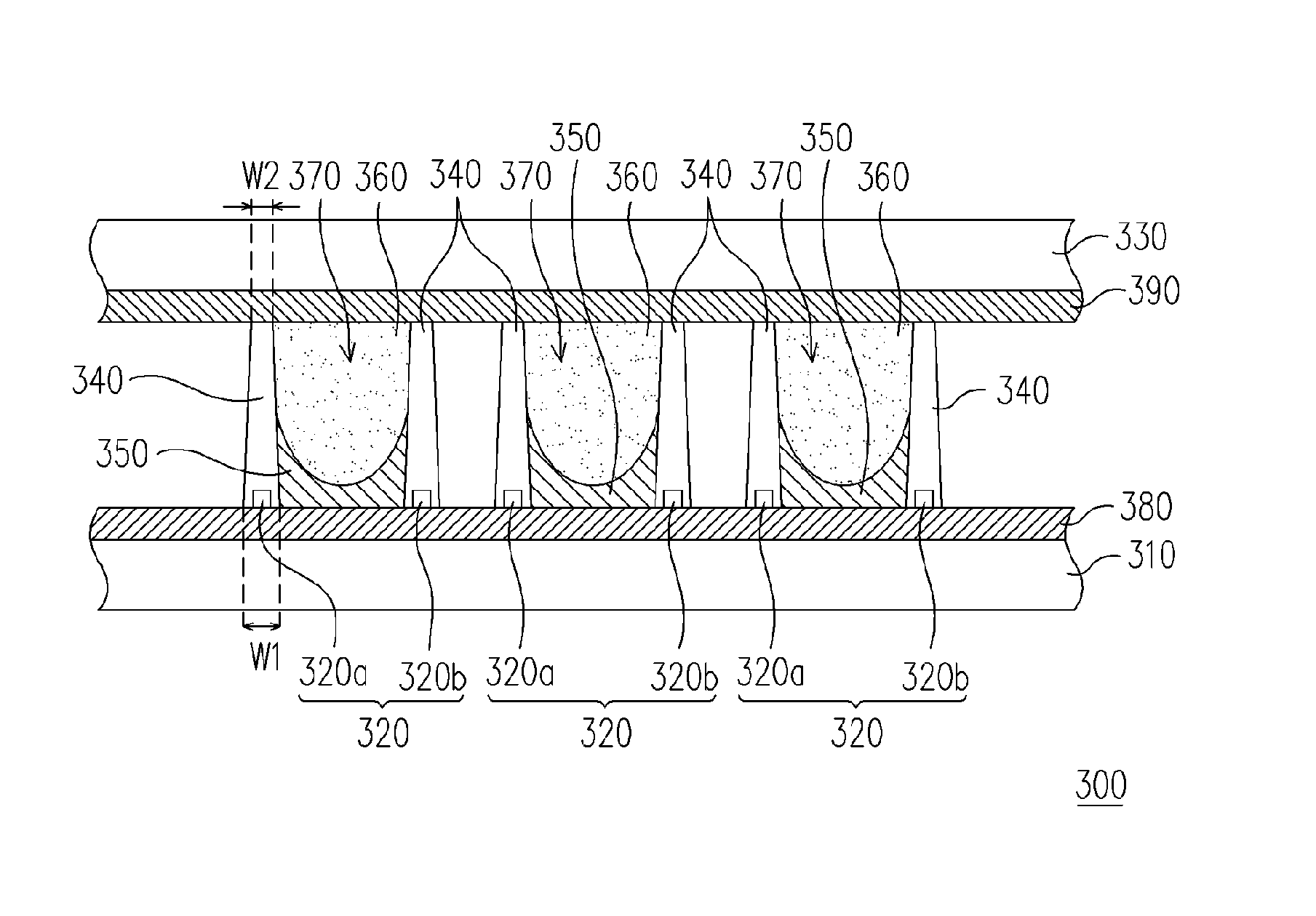
[0040]FIG. 3 is a diagram of a planar light source according to an embodiment of the present invention. Referring to FIG. 3, the planar light source 300 includes a first substrate 310, a plurality of electrode modules 320, a second substrate 330, a plurality of dielectric spacers 340, a phosphor layer 350, and a discharge gas 360. The electrode modules 320 are disposed on the first substrate 310. The second substrate 330 is disposed above the first substrate 310. The dielectric spacers 340 cover the electrode modules 320 and are connected between the first substrate 310 and the second substrate 330, and the space between the first substrate 310 and the second substrate 330 is divided into a plurality of discharge spaces 370 by the dielectric spacers 340. The phosphor layer 350 is disposed in the discharge spaces 370. The discharge gas 360 is disposed in the discharge spaces 370.

[0041] Referring to FIG. 3 again, in an embodiment, the first substrate 310 is, for example, a glass subs...


PUM


Abstract

A planar light source having a first substrate, a plurality of electrode modules, a second substrate, a dielectric spacer, a first phosphor layer, and a discharge gas is provided. The electrode modules are disposed on the first substrate. The second substrate is disposed above the first substrate. The dielectric spacer covers the electrode modules and is connected between the first substrate and the second substrate. The space between the first substrate and the second substrate is divided into a plurality of discharge spaces by the dielectric spacer. The first phosphor layer is disposed in the discharge spaces. The discharge gas is disposed in the discharge spaces. The coating area of the phosphor layer can be increased and cracks in the substrate can be prevented due to the simple structure of the planar light source.

Description

BACKGROUND OF THE INVENTION [0001] 1. Field of Invention [0002] The present invention relates to a planar light source and the fabricating method thereof. More particularly, the present invention relates to a planar light source with a simple structure and the fabricating method thereof with simplified process. [0003] 2. Description of Related Art [0004] The planar light source is widely used in the backlight of LCD display panels and even other fields because it has excellent light-emitting efficiency and evenness, and is capable of providing the light source for a large area. The planar light source is a kind of plasma light-emitting device, wherein, electrons emitted from the cathode will move between the cathode and the anode and collide with the inert gas in the discharge space so that the gas will be ionized and excited to form plasma. After that, the excited atoms in the plasma will degenerate into ground state with emitting Ultra-Violet, and the emitted ultra violet will fur...

Claims


Application Information

Patent Timeline
Patent Type & Authority Applications(United States)
IPC IPC(8): H01J17/49
CPCG02F1/133604H01J9/02H01J9/268H01J61/305H01J65/046
Inventor CHANG, CHAO-JENLEE, SU-CHIUTENG, HSIANG-HUIHSIEH, YU-HENGWU, HON-WE
Owner CHUNGHWA PICTURE TUBES LTD
Why Eureka
Try Eureka