Base panel having partition and plasma display device utilizing the same

a plasma display and base panel technology, applied in the direction of gas exhaustion means, discharge tubes luminescnet screens, electrodes, etc., can solve the problem of inability to fundamentally solve cross talk between adjacent pixels, discharge error, and difficulty in either supplying discharge gas from the discharge space partitioned by barriers or supplying discharge gas into, so as to improve the exhaust gas exhaustion efficiency and improve luminance. effect of luminan

Inactive Publication Date: 2005-01-11
SAMSUNG SDI CO LTD
View PDF7 Cites 5 Cited by
  • Summary
  • Abstract
  • Description
  • Claims
  • Application Information

AI Technical Summary

Benefits of technology

To solve the above and other problems, it is an object of the present invention to provide a base panel having a partition structure which can exhibit an improved level of luminance by increasing the coating area of a phosphor layer and which can improve the exhaustion efficiency of exhaust gas, and a plasma display device utilizing the base panel.

Problems solved by technology

Since the barriers surround every surface of a discharge space, it is difficult to either exhaust gas from the discharge space partitioned by the barriers or to inject discharge gas into the discharge space during the manufacture of the plasma display device.
However, the protrusion forming step is a separate process, and charges move through the gap formed between the barrier and the front substrate, which may cause a discharge error.
While these separator walls widen the discharge space to some extent, they cannot fundamentally solve the problem of cross talk between adjacent pixels.

Method used


Image

  • Base panel having partition and plasma display device utilizing the same
  • Base panel having partition and plasma display device utilizing the same
  • Base panel having partition and plasma display device utilizing the same

Examples


Embodiment Construction

Reference will now be made in detail to the present preferred embodiments of the present invention, examples of which are illustrated in the accompanying drawings, wherein like reference numerals refer to the like elements throughout. The embodiments are described below in order to explain the present invention by referring to the figures.

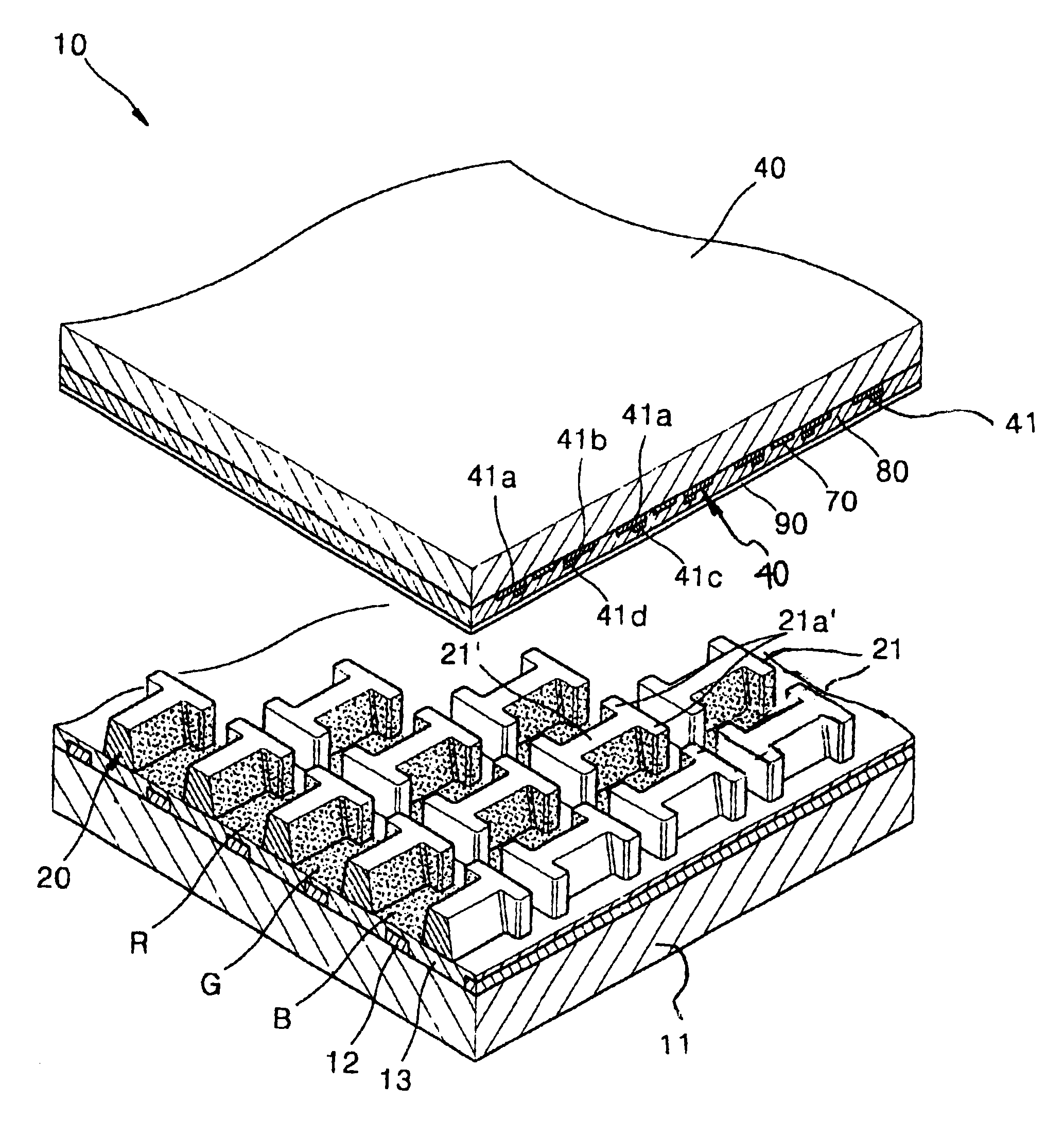
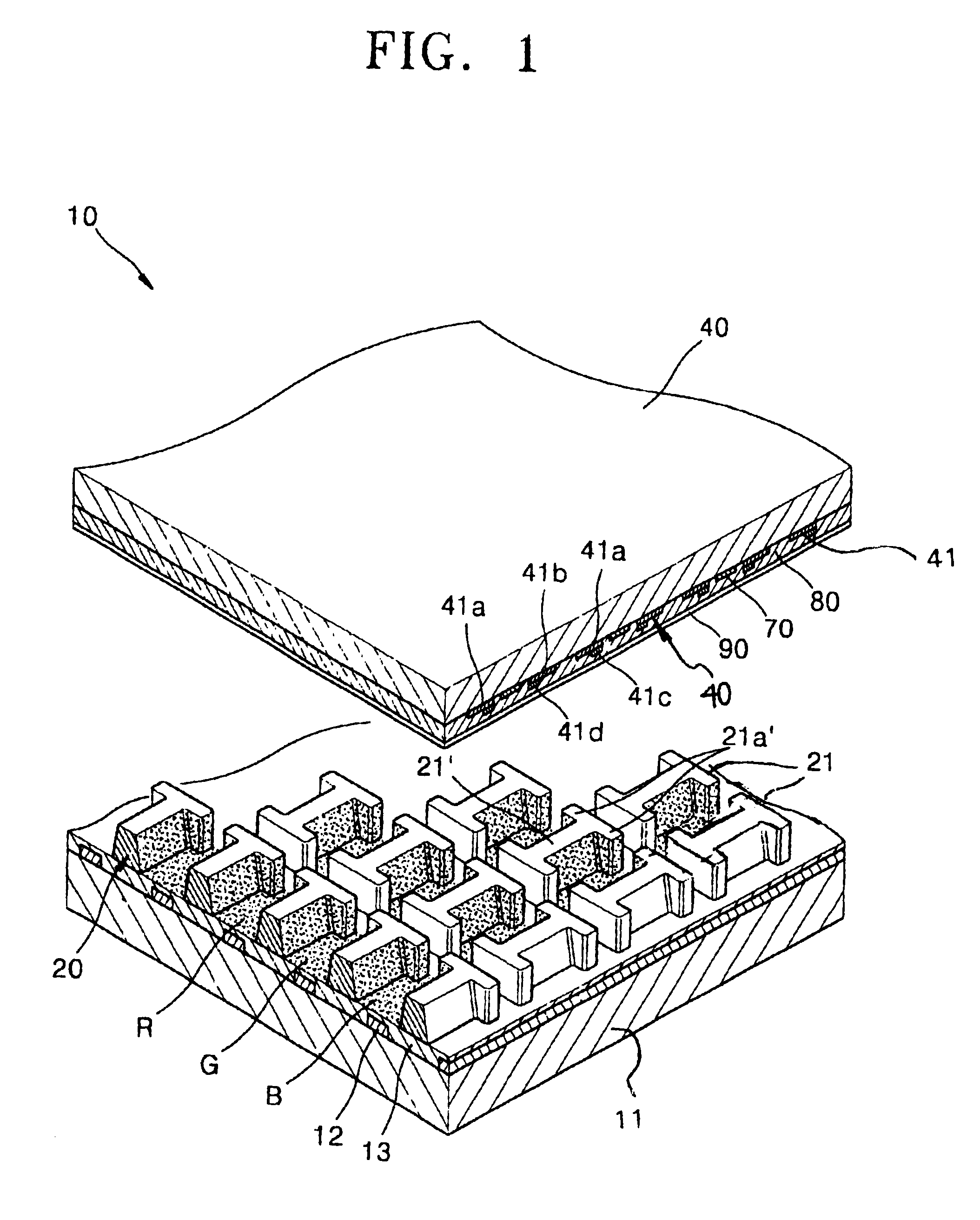
FIG. 1 shows a plasma display device 10 according to an embodiment of the present invention. As shown, the plasma display device 10 includes a first panel 11, address electrodes 12 formed on the first panel 11 in a predetermined pattern, and a first dielectric layer 13, formed on the first panel 11 covering the address electrodes 12. The address electrodes 12 are formed by stripes having predetermined widths and are parallel with each other. It is understood that the pattern of the address electrodes 12 is not limited to that shown by this embodiment.

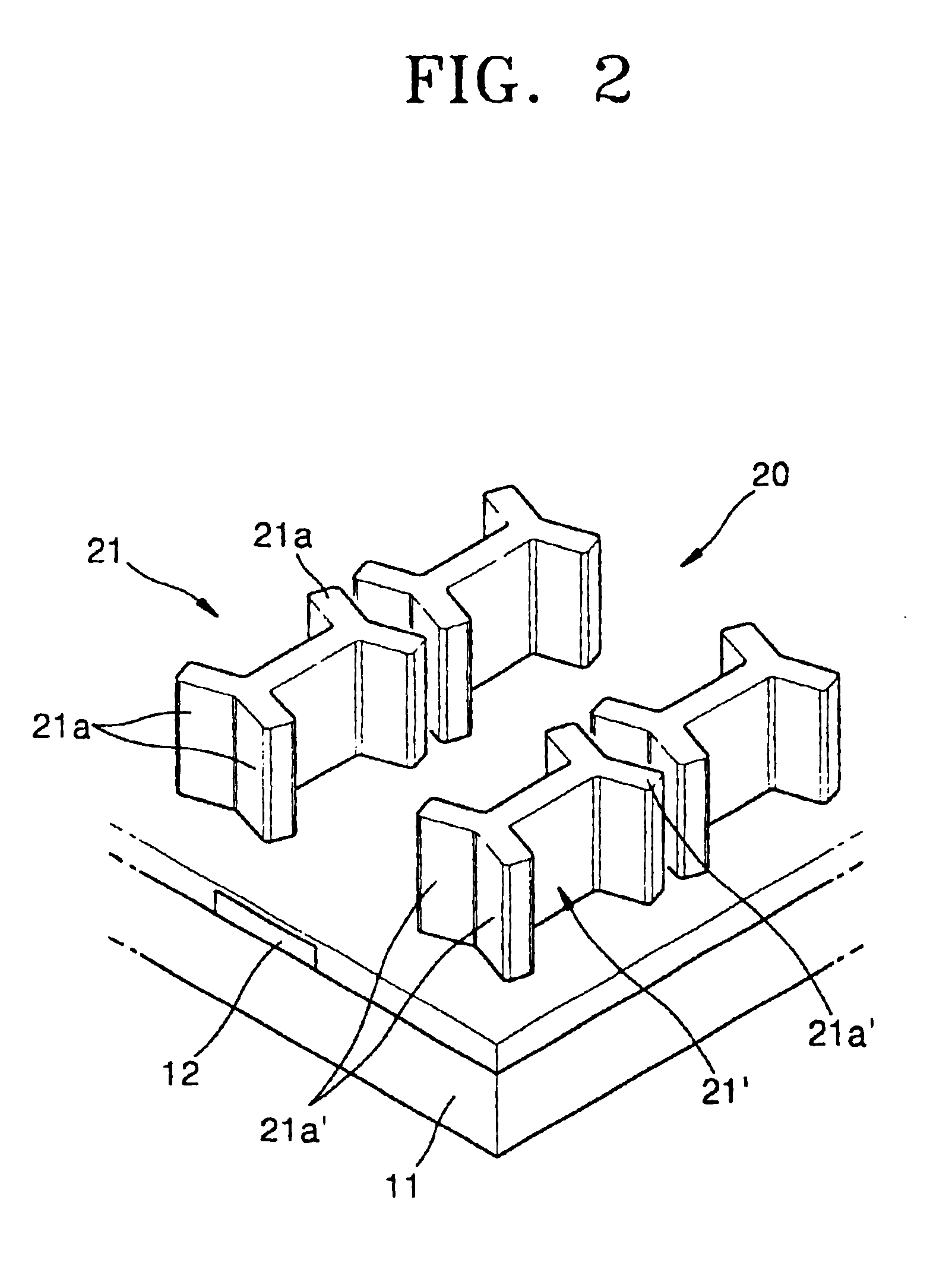
A partition structure 20, by which a discharge space is partitioned parallel to the direction of th...


PUM


Abstract

A plasma display panel including a first panel, address electrodes formed on the first panel in a predetermined pattern, a first dielectric layer formed on the first panel and covering the address electrodes, a partition structure having unit partitions discontinuously formed on the first dielectric layer to partition a discharge space, the unit partitions being parallel to the address electrodes and each having auxiliary partitions, red, green and blue phosphor layers coated in the partitioned discharge space, a second panel, which is coupled to the first panel to form the discharge space and which is transparent, a plurality of pairs of sustaining electrodes formed on an inner surface of the second panel and having sets of first and second electrodes at a predetermined angle with respect to the address electrodes, and a second dielectric layer formed on the second panel and covering the sustaining electrodes.

Description

BACKGROUND OF THE INVENTION1. Field of the InventionThe present invention relates to a plasma display device, and more particularly, to a base panel having a partition structure which can prevent cross talk between adjacent pixels, and a plasma display panel utilizing the base panel.2. Description of the Related ArtA plasma display panel generates light by exciting phosphors or a special gas, and using the reaction to form an image from the generated light. Plasma display panels are typically classified into an alternating current (AC) type, a direct current (DC) type, or a hybrid type.An AC plasma display device includes a base panel and a front panel. The base panel includes address electrodes formed thereon, a lower dielectric layer formed on the resultant structure having the address electrodes, and partitions, formed on the lower dielectric layer, to maintain a discharge gap and to prevent electrical and optical cross talk between cells defined between the partitions. The front...

Claims


Application Information

Patent Timeline
Patent Type & Authority Patents(United States)
IPC IPC(8): H01J17/02H01J17/16H01J11/12H01J11/22H01J11/24H01J11/26H01J11/34H01J11/36H01J11/44H01J11/54
CPCH01J11/12H01J11/36H01J11/54H01J2211/444H01J2211/365H01J9/24
Inventor KANG, TAE-KYOUNG
Owner SAMSUNG SDI CO LTD
Why Eureka
Try Eureka