Apparatus for dispensing photo-resist in semiconductor device fabrication equipment

a technology of semiconductor devices and apparatus, applied in the direction of liquid degasification, separation processes, coatings, etc., can solve the problems of increasing overall fabrication costs, too thin or overlapping photo-resist layers, and constant performance demands on the precision of conventional photolithography processes, so as to increase or maximize the productive yield of semiconductor devices and increase reliability.

Active Publication Date: 2007-05-31
SAMSUNG ELECTRONICS CO LTD
View PDF24 Cites 20 Cited by
  • Summary
  • Abstract
  • Description
  • Claims
  • Application Information

AI Technical Summary

Benefits of technology

[0018] Embodiments of the invention provide a photo-resist dispensing apparatus adapted to increase or maximize the productive yield of semiconductor devices by increasing the reliability with which gas bubbles are removed from a photo-resist solution delivered to an intermediate tank.

Problems solved by technology

This downward pressure on critical dimensions places constant performance demands upon the precision of conventional photolithography processes.
Where an insufficient volume of photo-resist is dispensed onto the center of the wafer the resulting photo-resist layer will be too thin or have gaps formed therein.
On the contrary, where an excessive volume of photo-resist is used the overall fabrication costs will rise as a large volume of photo-resist is wasted.
There are significant obstacles to the precision operation of a photo-resist dispensing apparatus.
For example, if the photo-resist being dispensed contains gas bubbles poor quality photo-resist layers will result.
An unstable or interrupted supply of photo-resist solution to the dispensing apparatus will also result in poor quality photo-resist layers.
Unfortunately, the conventional photo-resist dispensing apparatus suffers from a number of problems.
First, it has a disadvantage in that the photo-resist solution delivered within body 71 may pass from the inlet of supply line 43 to the output of supply line 43 without flowing through the bubble filter 73 configured in exhaust line 72.
This result yields unreliable results in the removal of bubbles.
In a related vein, the conventional photo-resist dispensing apparatus has the disadvantage of discharging bubbles not only through exhaust line 72, but also through the outlet of supply line 43 coupled to filter 5.
Any gas bubbles in the photo-resist solution will adversely effect the quality of wafer coating, and thus decreases a productive yield in the semiconductor devices being fabricated.

Method used


Image

  • Apparatus for dispensing photo-resist in semiconductor device fabrication equipment
  • Apparatus for dispensing photo-resist in semiconductor device fabrication equipment
  • Apparatus for dispensing photo-resist in semiconductor device fabrication equipment

Examples


Embodiment Construction

[0026] Exemplary embodiments of the invention are disclosed herein. However, the specific structural and functional details disclosed are merely representative and are presented as teaching examples. The invention may be variously embodied in many alternate forms and should not be construed as being limited to only the embodiments set forth herein.

[0027] Accordingly, while the invention is susceptible to various modifications and alternative forms, specific embodiments thereof are shown by way of example in the drawings and will herein be described in detail. It should be understood, however, that there is no intent to limit the invention to the particular forms disclosed, but on the contrary, the invention is to cover all modifications, equivalents, and alternatives falling within the spirit and scope of the invention. Like numbers refer to like elements throughout the description of the figures.

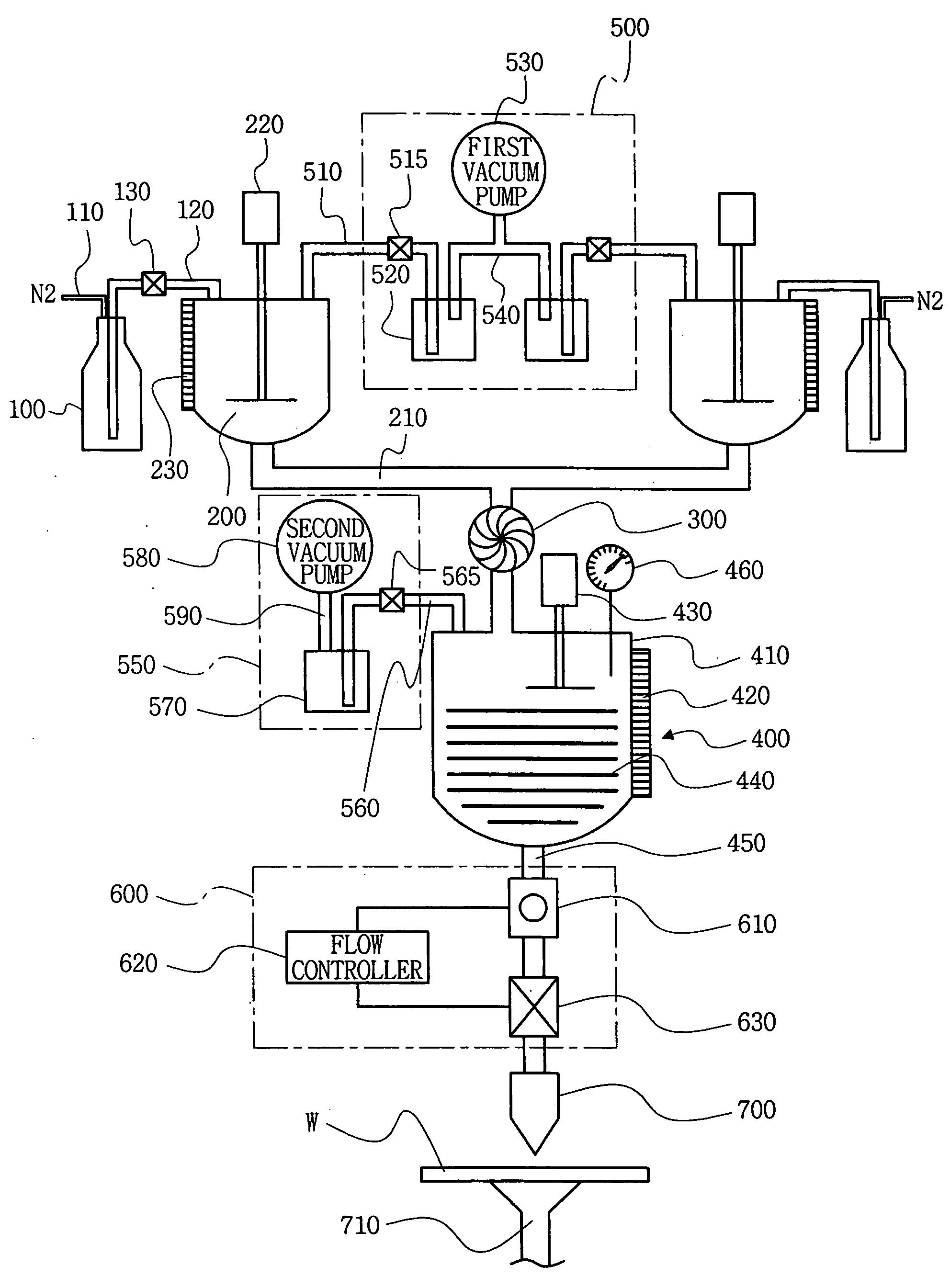
[0028]FIG. 3 is a schematic diagram illustrating a photo-resist dispensing apparatus ...


PUM

PropertyMeasurementUnit
pressureaaaaaaaaaa
rotary forceaaaaaaaaaa
pumping pressureaaaaaaaaaa

Abstract

A photo-resist dispensing apparatus is disclosed and comprises; a tank adapted to hold a photo-resist solution, a pump unit adapted to pump the photo-resist solution from the tank, a filter unit adapted to receive the photo-resist solution from the pump unit, and at least one of a first gas discharge unit connected to the tank and adapted to remove gas bubbles from the photo-resist solution held in the tank, and a second gas discharge unit connected to the filter unit and adapted to remove gas bubbles from the photo-resist solution in the filter.

Description

BACKGROUND OF THE INVENTION [0001] 1. Field of the Invention [0002] Embodiments of the present invention relate in general to the field of semiconductor device fabrication. More particularly, embodiments of the invention relate to an apparatus for dispensing a photo-resist in a uniformly coat on a semiconductor wafer. [0003] This application claims priority to Korean Patent Application No. 10-2005-0115742 filed on Nov. 30, 2005, the entire contents of which are hereby incorporated by reference. [0004] 2. Description of the Related Art [0005] Semiconductor devices are fabricated through the application of a complex sequence of individual processes. Very specialized fabrication equipment has been developed to perform these processes. Precision application of fabrication processes by this specialized equipment is critical to the ultimate quality of the semiconductor devices being fabricated. Many individual fabrication processes are repeatedly applied to a semiconductor wafer during th...

Claims


Application Information

Patent Timeline
Patent Type & Authority Applications(United States)
IPC IPC(8): B01D53/14
CPCB01D19/0036H01L21/67017H01L21/6715H01L21/67253
Inventor PARK, JIN-JUNYUN, SUK-FILL
Owner SAMSUNG ELECTRONICS CO LTD
Why Eureka
Try Eureka