Field-effect microelectronic device, capable of forming one or several transistor channels

a microelectronic device and field-effect transistor technology, applied in transistors, solid-state devices, electric devices, etc., can solve the problems of reducing the threshold voltage, affecting the good functioning of transistors, and increasing the leakage of transistors while off, so as to improve the field-effect transistor

Active Publication Date: 2007-06-07
COMMISSARIAT A LENERGIE ATOMIQUE ET AUX ENERGIES ALTERNATIVES
View PDF11 Cites 46 Cited by
  • Summary
  • Abstract
  • Description
  • Claims
  • Application Information

AI Technical Summary

Benefits of technology

[0017] This invention aims to present a field-effect microelectronic device comprising a structure forming one or more transistor channels. This structu

Problems solved by technology

This tendency can lead to effects that hinder the good functioning of transistors, such as “short channel effects”.
“Short channel effects” lead, among other things, to a reduction in the threshold voltage with the channel length and the drain voltage, which leads to an increase in leakage of the transistor while off.
This is hardly compatible with the improvement of the performance of integrated circuits.
The

Method used


Image

  • Field-effect microelectronic device, capable of forming one or several transistor channels
  • Field-effect microelectronic device, capable of forming one or several transistor channels
  • Field-effect microelectronic device, capable of forming one or several transistor channels

Examples


Embodiment Construction

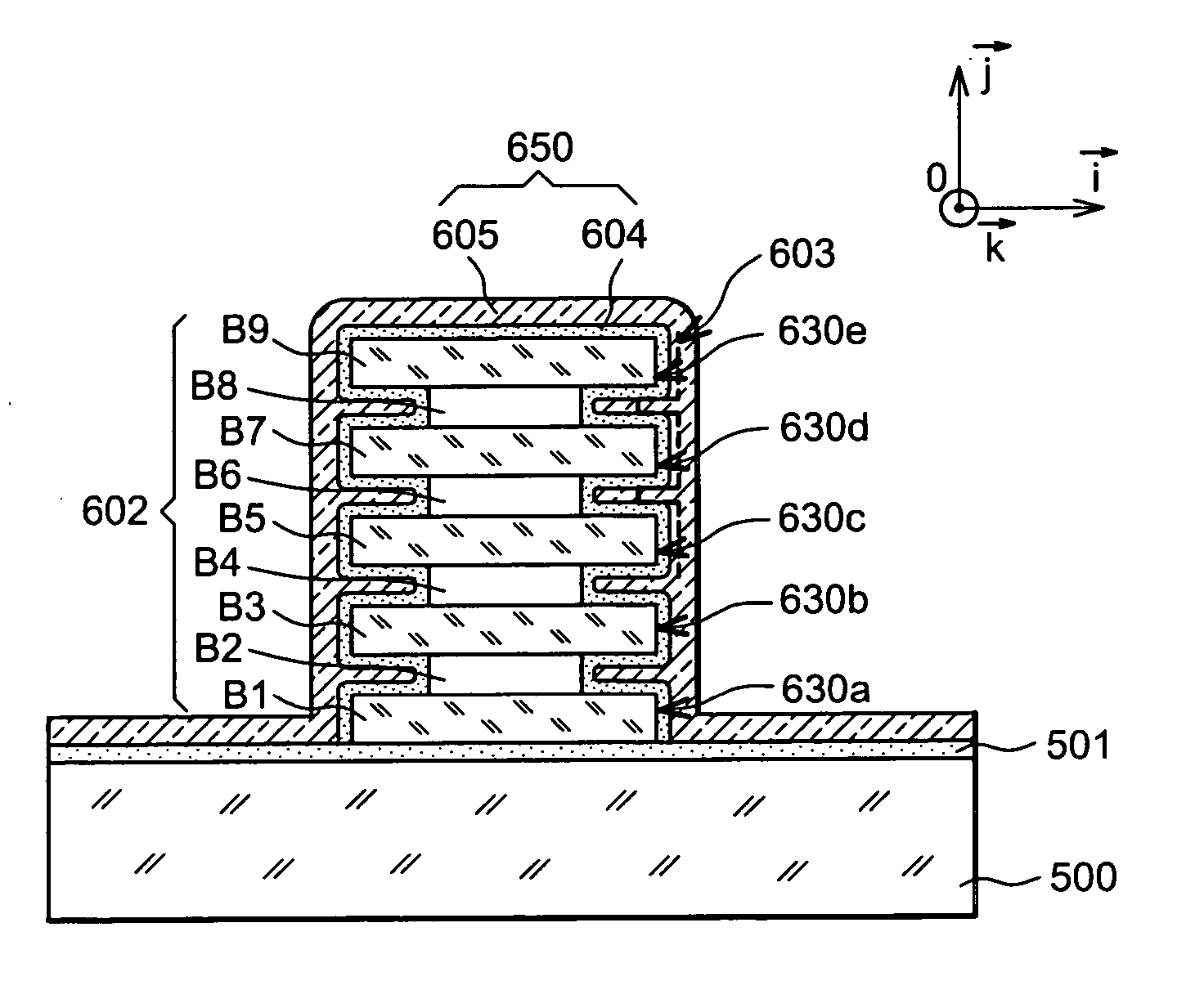
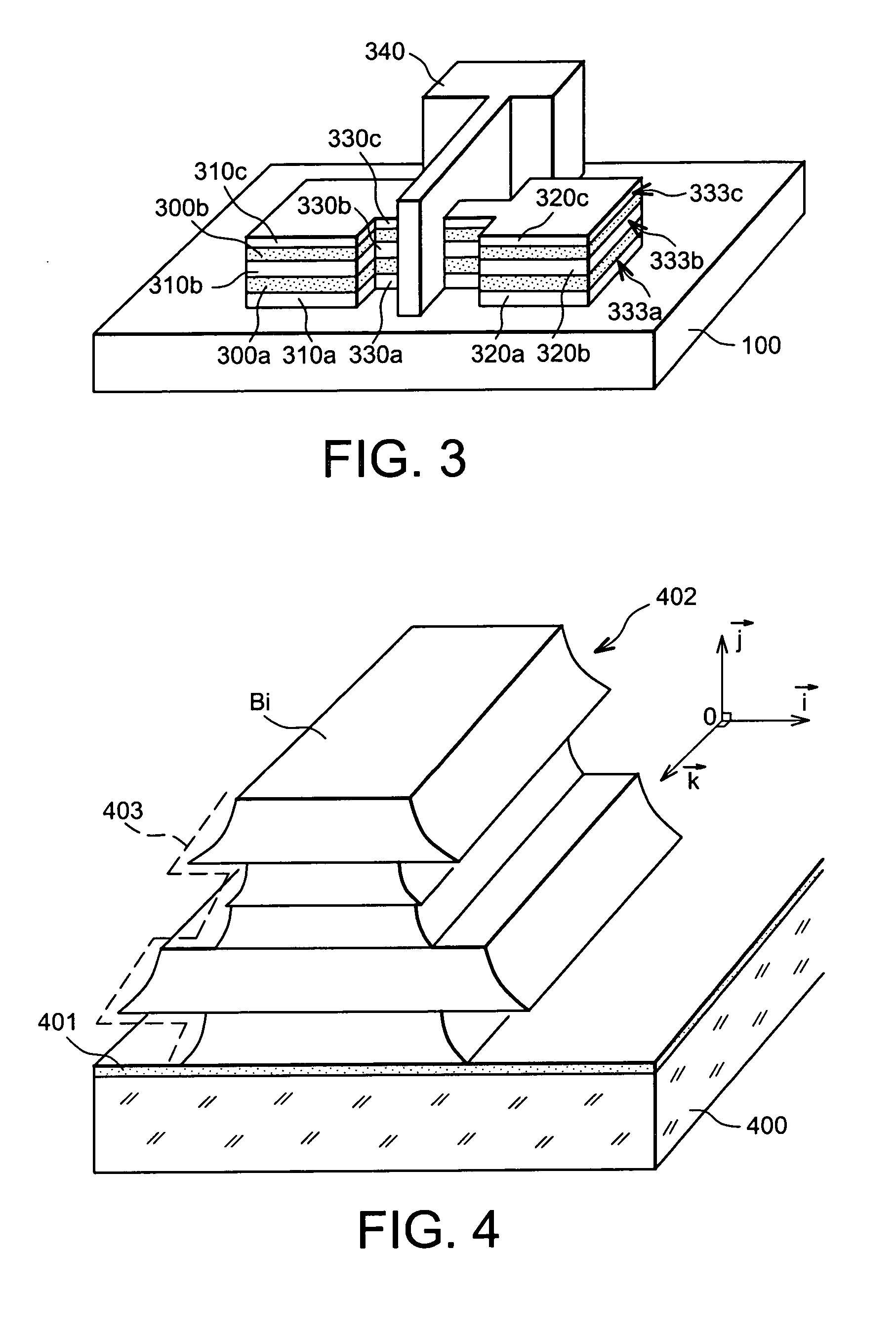
[0070]FIG. 4 shows an example of a microelectronic device according to the invention. It shows a substrate 400, for example, based on a semiconductive material, covered with an insulating layer 401. A structure 402 rests on the substrate 400. It is formed as a stack, in a direction orthogonal to a main plane of the substrate 400, of a plurality of bars Bi, based, for example, on a semiconductive material.

[0071] The term main plane of the substrate 400 refers to a plane parallel to the surface of the layer 401, or passing through the substrate 400 and parallel to a plane [O; {right arrow over (i)}; {right arrow over (k)}] of an orthogonal reference [O; {right arrow over (i)}; {right arrow over (j)}; {right arrow over (k)}] shown in FIG. 4.

[0072] This device can be obtained using thin layer production methods. The term bar refers to blocks, zones or blades with substantially parallelepipedic shapes extracted from thin films.

[0073] The bars are obtained, for example, by etching thin...


PUM


Abstract

The invention relates to a field-effect microelectronic device, as well as the method of production thereof. The device includes a substrate (700) as well as at least one improved structure (702) capable of forming one or more transistor channels. This structure, formed by a plurality of bars stacked on the substrate, can make it possible to save space in the integration of field-effect transistors as well as to improve the performance thereof.

Description

TECHNICAL FIELD AND PRIOR ART [0001] This invention relates to the field of integrated circuits, and more specifically to field-effect transistors. [0002] A known field-effect transistor structure 111 is shown in FIG. 1. It includes a first area forming a source 110, a second area forming a drain 120 and rests on a substrate 100 for example based on silicon. [0003] The source 110 and the drain 120 have a substantially rectangular shape and are partially flush with the surface of the substrate 100. The transistor structure 111 also comprises a channel in the form of a block or bar, with a shape similar to that of a parallelepiped, and enabling the source 110 and the drain 120 to be connected in the direction of its length. The channel has a length L measured in a source-drain direction as well as a width W measured in a direction parallel to a main plane of the substrate 100. [0004] The channel is covered by a zone forming a gate 140. The gate 140 is in contact with the channel over ...

Claims


Application Information

Patent Timeline
IPC IPC(8): H01L29/76H01L21/336H01L29/423H01L29/786
CPCH01L29/42384H01L29/66742H01L29/66795H01L29/7853H01L29/78687
Inventor ERNST, THOMASBOREL, STEPHAN
Owner COMMISSARIAT A LENERGIE ATOMIQUE ET AUX ENERGIES ALTERNATIVES
Why Eureka
Try Eureka