Solder alloy, solder ball, and solder joint using the same
a technology of solder ball and alloy, which is applied in the direction of soldering apparatus, manufacturing tools, and capacitors, can solve the problems of increasing melting point and thermal damage to semiconductor packages, and achieve the effect of suppressing a decrease in joint strength, reducing metallic luster, and not impairing the ductility of sn—cu alloy
- Summary
- Abstract
- Description
- Claims
- Application Information
AI Technical Summary
Benefits of technology
Problems solved by technology
Method used
Image

Examples
example 2
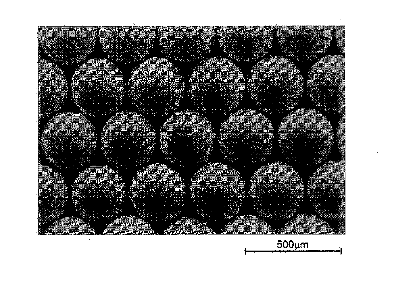
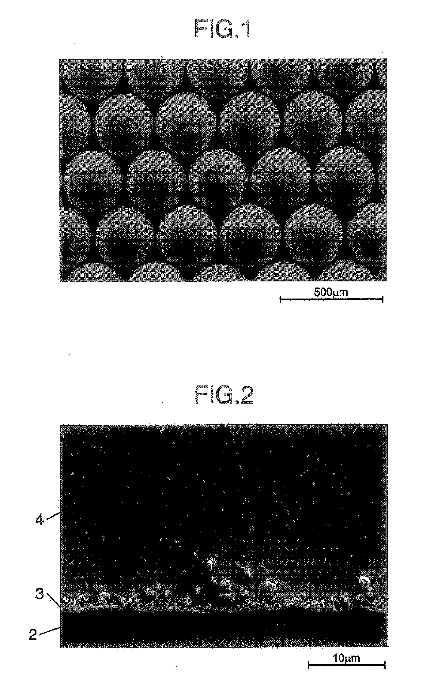
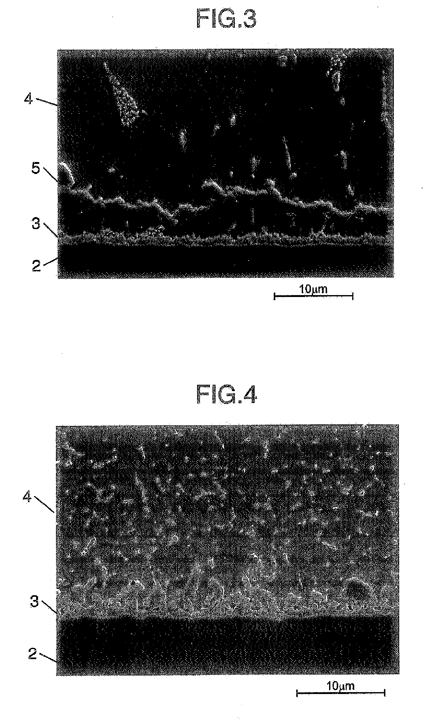
[0055] Subsequently, solder balls having a diameter of 0.3 mm were used to form solder bumps on an electrode (referred below to as Ni electrode), which was provided by performing electrolytic Ni / Au plating on a Cu substrate, and reliability in solder joint was evaluated. The electrode had a diameter of 0.25 mm. Soldering was performed by heating to 240° C. and in order to evaluate a deterioration behavior in high-temperature environment, samples, which were annealed at 150° C. for 100 hours after soldering, were also fabricated. With respect to the samples fabricated in this manner, spalling of a Cu—Ni—Sn compound formed on a joint interface was confirmed and a cross-sectional structure was observed for measurement of a thickness of the compound. An area of an interface compound in a cross-sectional structure photograph was measured by means of image processing, and a thickness of a Cu—Ni—Sn compound was calculated as a thickness per unit length of a joint interface. TABLE 3 indicat...
example 3
[0061] In order to evaluate a drop impact strength, bound-level drop test was carried out on the basis of the JEDEC Standards JESD22-B111. Test substrates for the drop test were fabricated by using solder balls having a diameter of 0.3 mm to form solder bumps on BGA having 345 Ni electrodes and then using a solder paste to join the solder bumps to a mother board.
[0062] Sn-3Ag-0.5Cu (by mass %) as generally used was used for the solder paste. Subsequently, after a test substrate was fixed horizontally to a drop table, it was dropped 30 times from a level, at which level a drop impact applied to the drop table was 1500 G to form a half-sine wave of 0.5 ms, while being maintained in a horizontal posture. In the drop test, bias of a daisy-chain circuit formed between BOA and the mother board was measured to find electrical failure. For respective compositions of solder, two test substrates, that is 30 BGAs in total, were evaluated, since 15 BGAs were mounted every test substrate.
[0063...
PUM
| Property | Measurement | Unit |
|---|---|---|
| Fraction | aaaaa | aaaaa |
| Fraction | aaaaa | aaaaa |
| Fraction | aaaaa | aaaaa |
Abstract
Description
Claims
Application Information
 - R&D Engineer
- R&D Manager
- IP Professional
- Industry Leading Data Capabilities
- Powerful AI technology
- Patent DNA Extraction
Browse by: Latest US Patents, China's latest patents, Technical Efficacy Thesaurus, Application Domain, Technology Topic.
© 2024 PatSnap. All rights reserved.Legal|Privacy policy|Modern Slavery Act Transparency Statement|Sitemap