Semiconductor device

a technology of semiconductor devices and semiconductors, applied in the direction of semiconductor devices, basic electric elements, electrical equipment, etc., can solve the problems of increasing resistance, power consumption, resistance and resistance in the element, and deteriorating breakdown voltag

Inactive Publication Date: 2007-06-28
KK TOSHIBA
View PDF5 Cites 45 Cited by
  • Summary
  • Abstract
  • Description
  • Claims
  • Application Information

AI Technical Summary

Problems solved by technology

In such the trench-gate structure, electric field concentration may easily arise at a corner of the bottom of the trench and this may cause deterioration of the breakdown voltage as a problem.
If the radius of curvature at the trench corner is small, current flows in a drift layer not uniformly, thereby increasing the drift resistance, resulting in increases in on resistance and power consumption in the element as a problem.
Accordingly, this causes an increase in on resistance as a problem.
The void easily occurs in the reverse-tapered trench though the same problem arises if a void occurs regardless of the trench shape.
Such the migration of the void may cause the following two problems associated with the reliability of the gate electrode.
One is a problem found in a gate ruggedness test because an electric field concentrates on the gate insulator at a void edge (a boundary between the void and the polysilicon).
Another is a problem related to the above electric field concentration that facilitates charges to flow through the gate insulator.

Method used


Image

  • Semiconductor device
  • Semiconductor device
  • Semiconductor device

Examples


Embodiment Construction

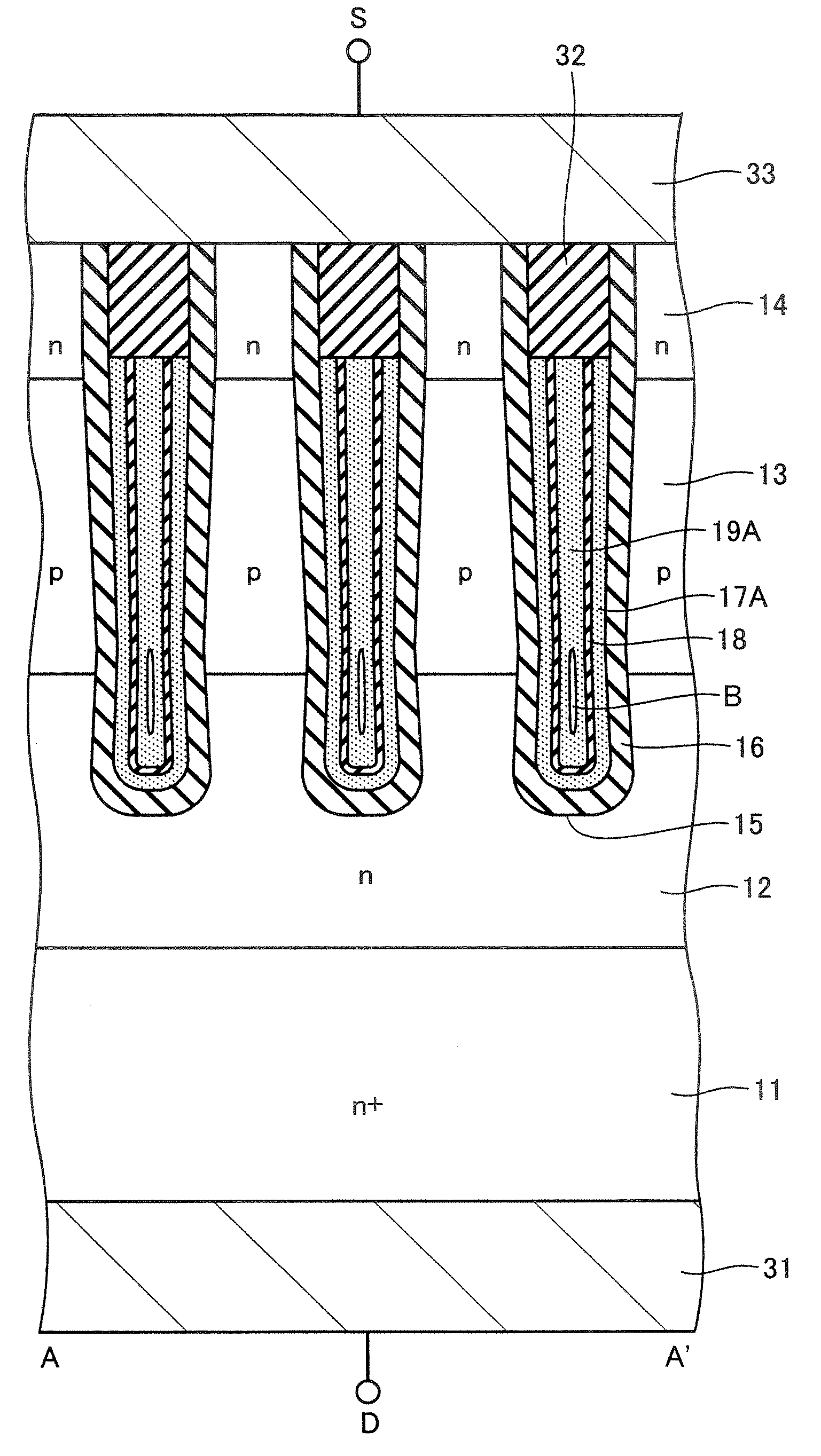
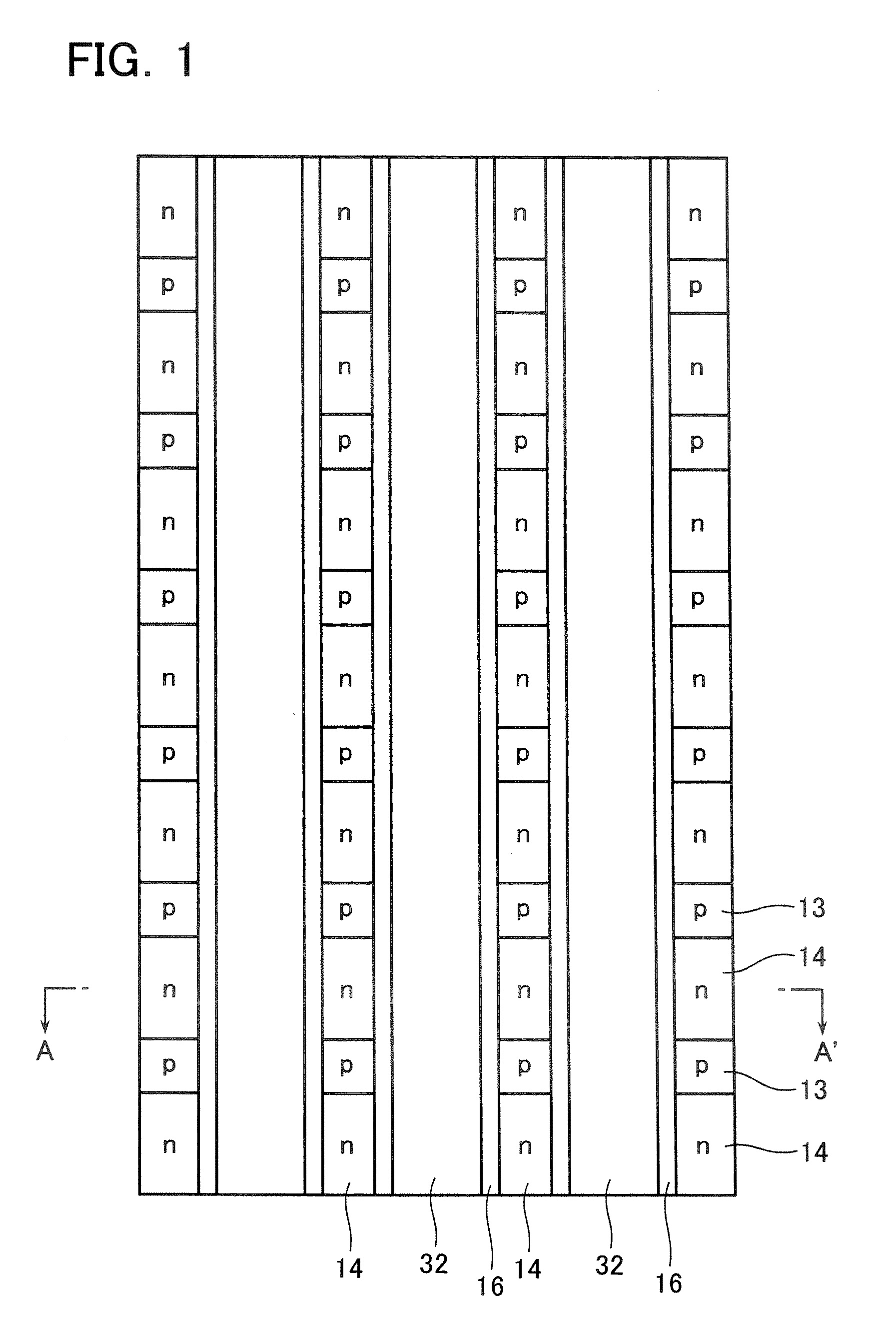
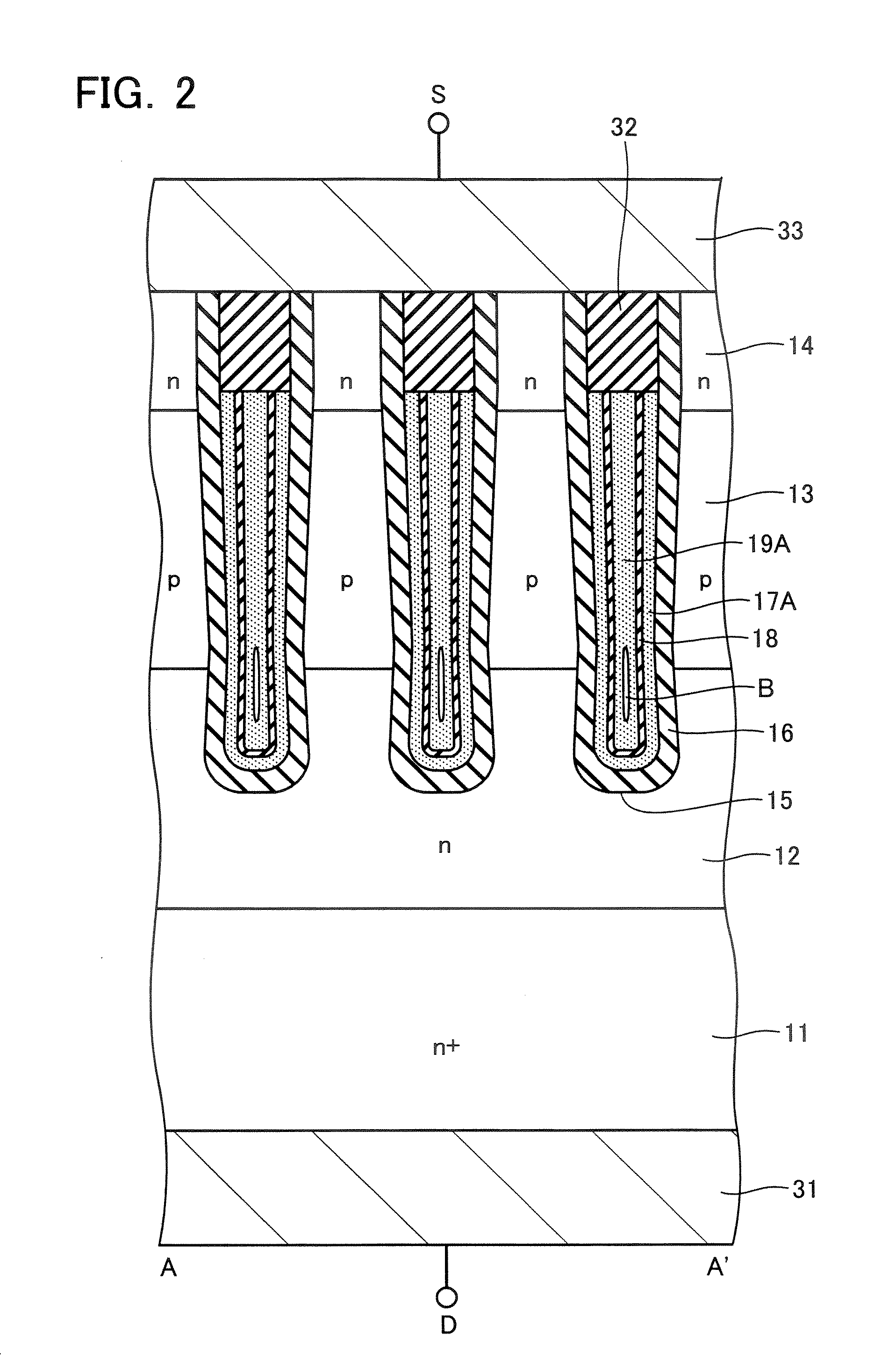
[0018] Semiconductor devices according to the embodiments of the present invention will now be described next in detail with reference to the drawings. FIG. 1 shows a plan view of a semiconductor device according to a first embodiment of the present invention, and FIG. 2 shows an A-A′ cross-sectional view thereof. FIG. 1 shows a plan view in a state where a later-described source electrode 33 is removed. In the following embodiments, with the first and second conduction types exemplified as the n-type and p-type, an n-channel MOS transistor having a p-type base layer is shown.

[0019] As shown in FIG. 2, the n-channel MOS transistor comprises an n+-type silicon substrate 11. The n+-type silicon substrate 11 serves as a drain layer connected to a drain electrode 31 on the rear surface. Formed on the silicon substrate 11 is an n-type drift layer 12 having a lower impurity concentration and a higher resistance than those of the silicon substrate 11, and a p-type base layer 13 is formed ...


PUM


Abstract

A semiconductor device comprises on a surface of a first semiconductor layer of the first conduction type a second semiconductor layer of the first conduction type. A semiconductor base layer of the second conduction type is formed on the second semiconductor layer, and a semiconductor diffusion layer of the first conduction type is formed on a surface of the semiconductor base layer. A trench is formed from the surface of the semiconductor diffusion layer to a depth reaching the second semiconductor layer. A gate electrode is formed of a conductor film buried in the trench with a gate insulator interposed therebetween. The conductor film includes a first conductor film formed along the gate electrode to have a recess and a second conductor film formed to fill the recess.

Description

CROSS REFERENCE TO RELATED APPLICATION [0001] This application is based on and claims the benefit of priority from prior Japanese Patent Application No. 2005-377841, filed on Dec. 28, 2005, the entire contents of which are incorporated herein by reference. BACKGROUND OF THE INVENTION [0002] 1. Field of the Invention [0003] The present invention relates to a semiconductor device, and more particularly to a trench-gate semiconductor device. [0004] 2. Description of the Related Art [0005] Known power semiconductor elements capable of achieving a low on resistance include a trench-gate MOS transistor and an insulated-gate bipolar transistor (IGBT). [0006] A trench-gate, n-channel MOS transistor, for example, includes trenches formed in stripes or mesh such that they extend from an n-type source layer through a p-type base layer located below the source layer. A film of conductor such as polysilicon is buried with a gate insulator on a trench wall to form a gate electrode. Such the struc...

Claims


Application Information

Patent Timeline
Patent Type & Authority Applications(United States)
IPC IPC(8): H01L29/76
CPCH01L29/0649H01L29/0696H01L29/4236H01L29/42372H01L29/4925H01L29/4958H01L29/7397H01L29/7813
Inventor OHTA, TSUYOSHITANAKA, BUNGO
Owner KK TOSHIBA
Why Eureka
Try Eureka