Eureka AIR delivers breakthrough ideas for toughest innovation challenges, trusted by R&D personnel around the world.

Semiconductor package structure with constraint stiffener for cleaning and underfilling efficiency

a technology of constraint stiffener and packaging structure, which is applied in the direction of semiconductor devices, semiconductor/solid-state device details, electrical apparatus, etc., can solve the problems of significant thermally induced stress, space or gap between significant difference in the dimension of the chip and the substrate, so as to facilitate the egress of the dispenser

Inactive Publication Date: 2007-06-28
TAIWAN SEMICON MFG CO LTD
View PDF12 Cites 45 Cited by
  • Summary
  • Abstract
  • Description
  • Claims
  • Application Information

AI Technical Summary

Benefits of technology

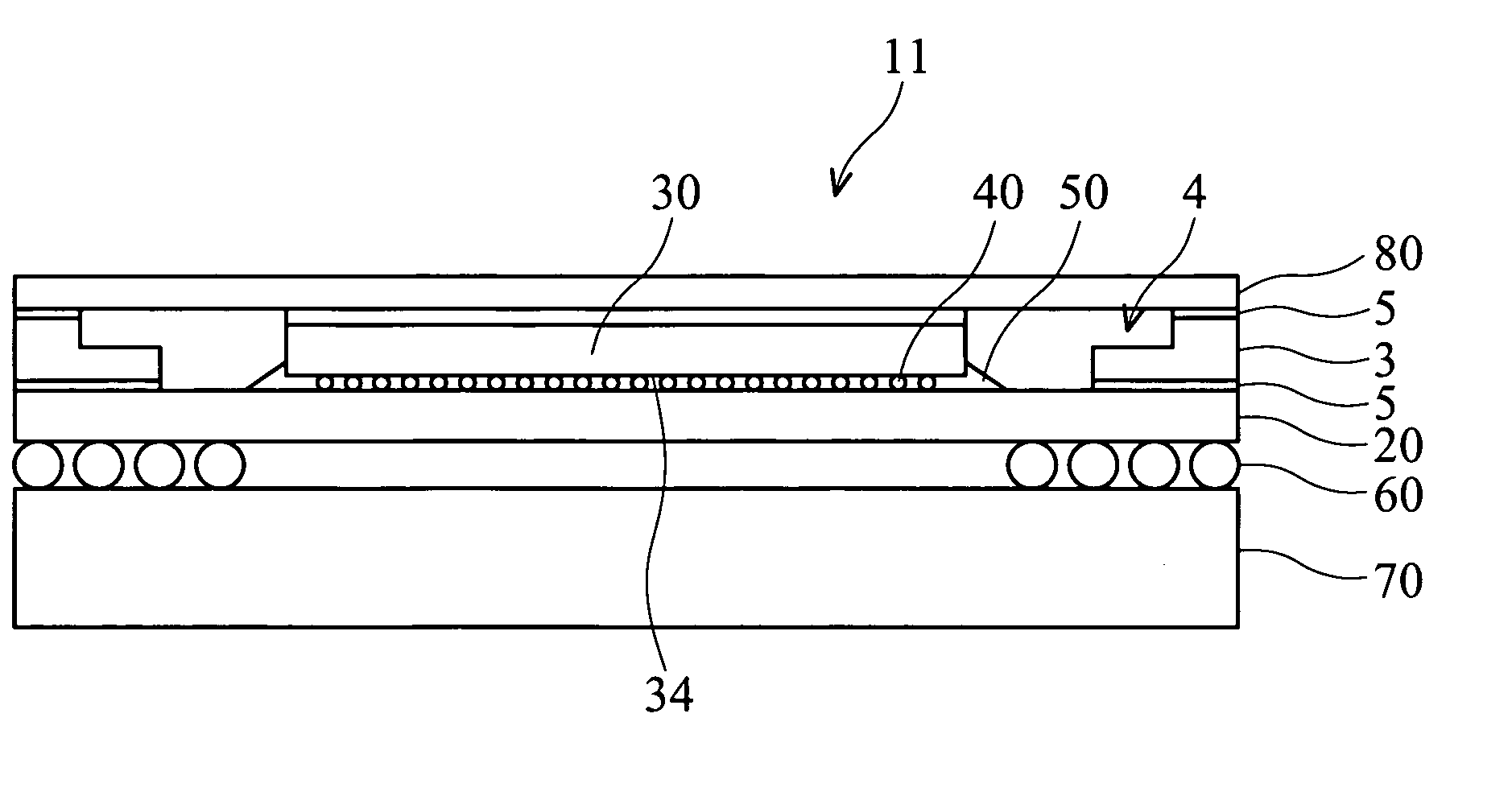
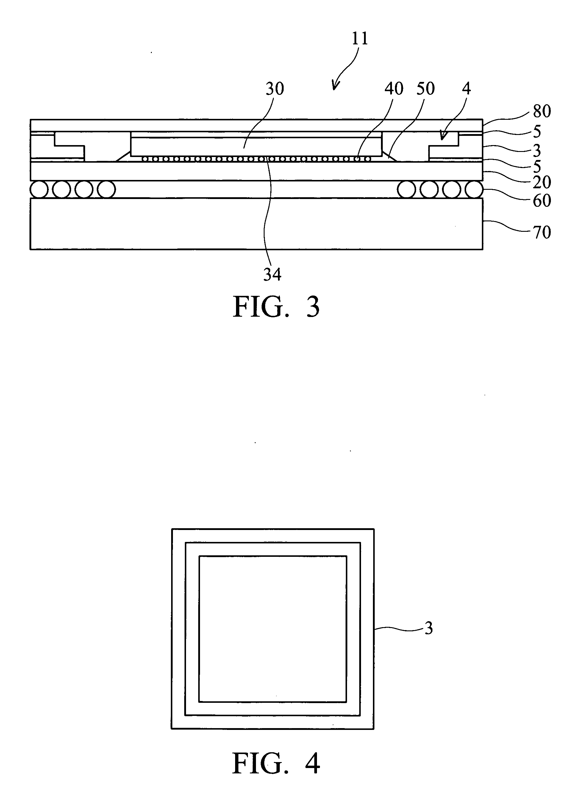
[0009] The present invention is directed to a semiconductor package structure with a heat dissipating stiffener and method of fabricating the same. In one embodiment, the package structure comprises a substrate having a front side and a back side; a semiconductor chip mounted on the front surface of the substrate; a thermally-conductive stiffener mounted over the front surface of the substrate and surrounding the chip, the stiffener having a first portion and a second portion, wherein the first portion is wider than the second portion so as to allow for easy egress of a dispenser into a gap between the chip and the substrate; an underfill layer filled and cured in the gap; and a plurality of solder balls mounted on the back surface of the substrate.

Problems solved by technology

The process of flip chip mounting results in a space or gap between the chip and the substrate.
As a result, the chip and the substrate experience significantly different dimension changes when heated that creates significant thermally-induced stresses in the electrical connections between the chip and the substrate.
If uncompensated, the disparity in thermal expansion can result in degradation in the performance of the chip, damage to the solder joints, or package failure.
As the size of the chip increases, the effect of a mismatch in the coefficient of thermal expansion between the chip and the substrate becomes more pronounced.
The failure mechanism in stacked die packages may shift from solder joint damage to die damage.
As a result, the underfill significantly increases the lifetime of the assembled package.
However, a drawback is that the cleaning solvent would be partly obstructed by the stiffener, making the cleaning process very difficult to carry out efficiently and thoroughly.
When some solder flux is still left, it would cause the subsequently formed flip chip underfill layer to have voids, which would considerably degrade the quality and reliability of the finished package product.
Another drawback to the conventional package assembly is that during the time the underfill is injected in the gap between the chip and the substrate, the underfill dispenser will be partly obstructed by the stiffener, making the underfill dispensing process a time consuming task and not easy to carry out thoroughly.

Method used


Image

  • Semiconductor package structure with constraint stiffener for cleaning and underfilling efficiency
  • Semiconductor package structure with constraint stiffener for cleaning and underfilling efficiency
  • Semiconductor package structure with constraint stiffener for cleaning and underfilling efficiency

Examples


Embodiment Construction

[0016] In the following description, numerous specific details are set forth to provide a thorough understanding of the present invention. However, one having an ordinary skill in the art will recognize that the invention can be practiced without these specific details. In some instances, well-known structures and processes have not been described in detail to avoid unnecessarily obscuring the present invention.

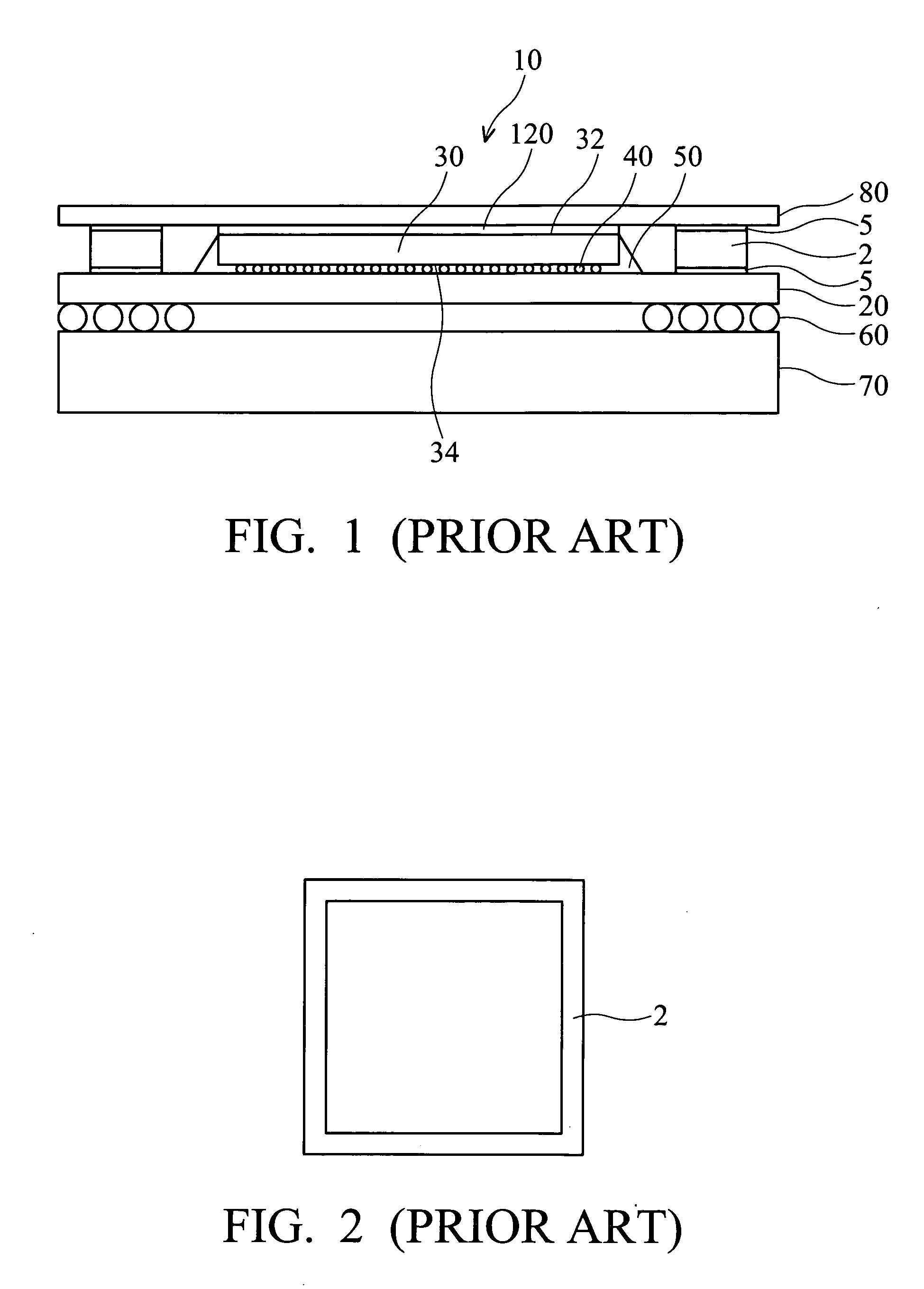
[0017]FIG. 1 is a cross-sectional view of a conventional semi-finished flip chip package showing a stiffener mounted to a substrate. Flip chip package 10 includes a chip 30 having an upper surface 32 and a lower surface 34 opposite the upper surface 32. A set of solder bumps 40 is connected to contact pads (not shown) on the lower surface 34 of chip 30. Chip 30 is secured to a first substrate 20 underlying chip 30. Solder bumps 40 are attached to contact pads (not shown) on an upper surface of first substrate 20. An underfill 50 may be filled between chip 30 and first substr...


PUM


Abstract

A semiconductor package structure with a heat dissipating stiffener and method of fabricating the same are provided. In one embodiment, the package structure comprises a substrate having a front side and a back side; a semiconductor chip mounted on the front surface of the substrate; a thermally-conductive stiffener mounted over the front surface of the substrate and surrounding the chip, the stiffener having a first portion and a second portion, wherein the first portion is wider than the second portion so as to allow for easy egress of a dispenser into a gap between the chip and the substrate; an underfill layer filled and cured in the gap; and a plurality of solder balls mounted on the back surface of the substrate.

Description

BACKGROUND [0001] The present invention relates generally to the fabrication of semiconductor chip packages, and more particularly, to a semiconductor package structure having a constraint stiffener for efficient cleaning and underfilling of a chip mounted on a substrate. [0002] In the microelectronics industry, a chip carrying an integrated circuit is commonly mounted on a package carrier, such as a substrate, a circuit board or a leadframe, that provides electrical connections from the chip to the exterior of the package. In one such packaging arrangement called flip chip mounting, the chip includes an area array of electrically conductive contacts, known as bond pads, that are electrically connected to corresponding area array of electrically-conductive contacts on the substrate, known as solder balls or bumps. Typically, the solder bumps are registered with the bond pads and a reflow process is applied to create electrical connections in the form of solder joints between the chi...

Claims


Application Information

Patent Timeline
IPC IPC(8): H01L23/34
CPCH01L21/52H01L21/563H01L23/04H01L23/36H01L24/28H01L24/81H01L2224/16225H01L2224/73203H01L2224/73204H01L2224/73253H01L2224/8121H01L2224/81815H01L2224/83102H01L2224/92125H01L2924/01005H01L2924/01029H01L2924/14H01L2924/15311H01L2924/16195H01L2924/3511H01L2924/01033
Inventor LEE, CHIEN-HSIUNHSIAO, YK
Owner TAIWAN SEMICON MFG CO LTD
Why Eureka
Eureka Blog
Learn More