Package structure of image sensor device

a technology of image sensor and package, applied in the direction of electrical equipment, instruments, electric discharge lamps, etc., can solve the problems of short circuits, electrical short circuits, and inability to efficiently reduce the thickness of the image sensor package, and achieve the effect of improving the thermal dissipation of the image sensor chip 120 and high fluidity

Inactive Publication Date: 2007-07-05
CHIPMOS TECH INC
View PDF5 Cites 28 Cited by
  • Summary
  • Abstract
  • Description
  • Claims
  • Application Information

AI Technical Summary

Benefits of technology

[0004] The main purpose of the present invention is to provide an image sensor package in which an image sensor chip is flip-chip mounted on a flexible circuit on a transparent carrier or a glass substrate, and a substrate cover is mounted on the flexible circuit / glass substrate. The substrate cover has a chip cavity and a plurality of electrical terminals. When disposition of the substrate cover, the chip cavity will accommodate the image sensor chip and the terminals of the substrate cover are electrically connected to the image sensor chip by the flexible circuit / glass substrate to replace the conventional bonding wires in the chip cavity. The image sensor package can meet the development of miniaturization with excellent protection of the image sensor chip.
[0005] The secondary purpose of the present invention is to provide an image sensor package in which an annular gap is formed between the substrate cover and the image sensor chip to prevent a liquid sealant from wetting the image sensor chip. The liquid sealant such as underfill material is formed between the substrate cover and the flexible circuit / glass substrate, can be used for hermetically sealing the image sensor chip without contaminating a sensing area of the image sensor chip.
[0006] The third purpose of the present invention is to provide an image sensor package in which the spacing between the substrate cover and the flexible circuit / glass substrate is smaller than that between the image sensor chip and the flexible circuit / glass substrate. The liquid sealant is formed between the substrate cover and the flexible circuit / glass substrate, can be used for hermetically sealing the image sensor chip without contaminating the image sensor chip.

Problems solved by technology

Therefore, the thickness of an image sensor package cannot efficiently be reduced.
However, during the packaging processes, the protrusion layer has to be formed on top of the substrate to form the chip cavity, which is very complicated.
When the light-transmission layer is attached to the protrusion layer, the bonding wires will be damaged resulting in electrical short or open.

Method used


Image

  • Package structure of image sensor device
  • Package structure of image sensor device
  • Package structure of image sensor device

Examples


Embodiment Construction

[0012] Please refer to the attached drawings, the present invention will be described by means of embodiment(s),below.

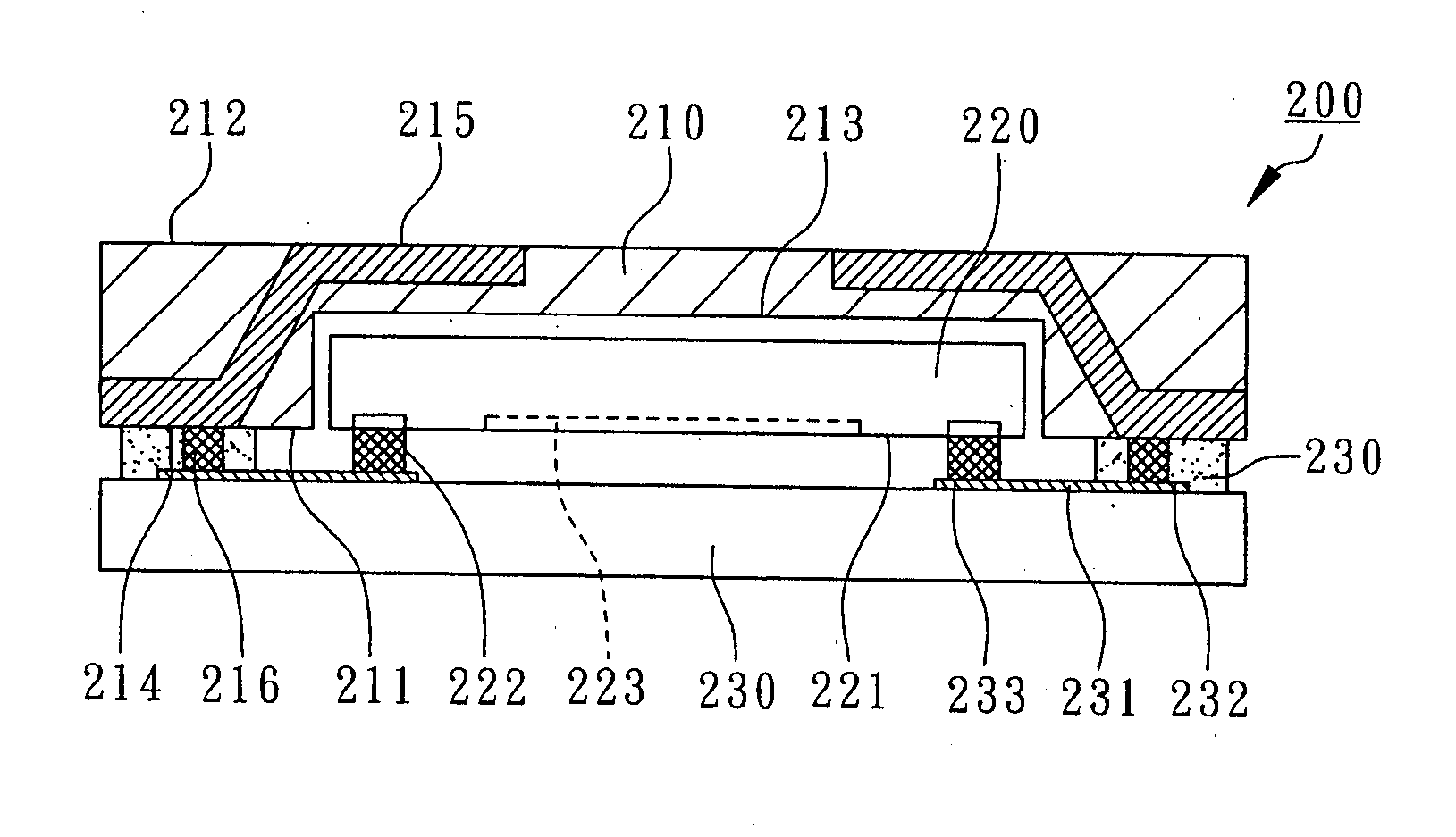
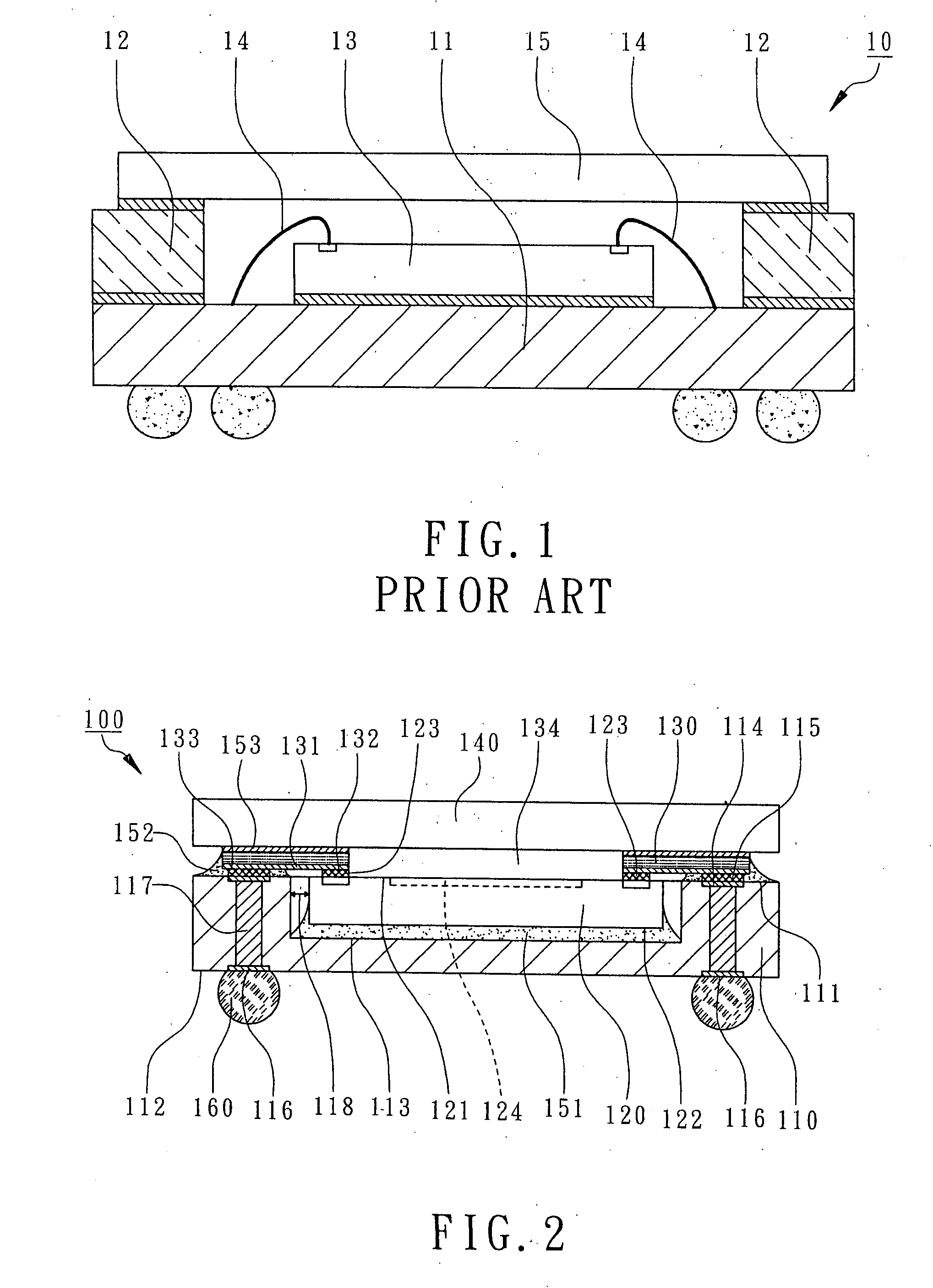
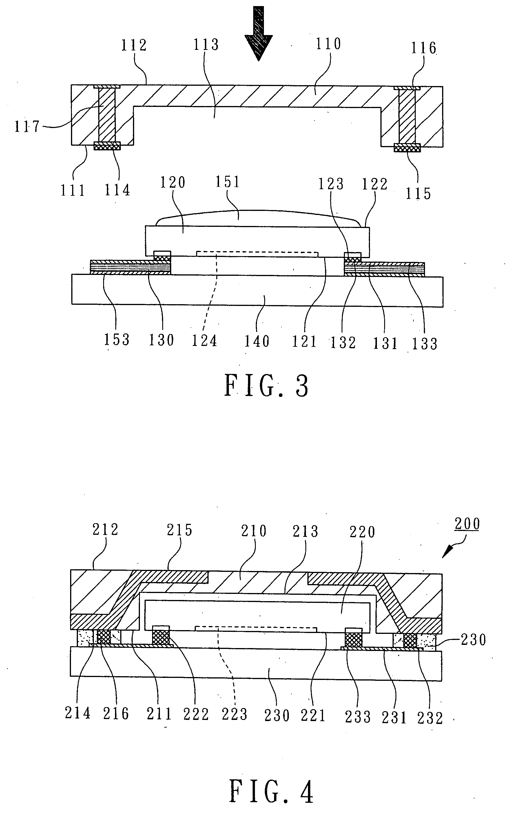
[0013]FIG. 2 shows an image sensor package 100 according to the first embodiment of the present invention, the package 100 comprises a substrate cover 110, an image sensor chip 120, a flexible circuit 130, and a transparent carrier 140. The transparent carrier 140 is rigid for attaching the flexible circuit 130 and flip-chip mounting. Preferably, the transparent carrier 140 is an optical glass.

[0014] The flexible circuit 130 is attached to the transparent carrier 140 by adhesive 153. The flexible circuit 130 may be selected from a COF (Chip-On-Film) tape, a TCP (Tape Automated Package) tape, or a high-density FPC. The flexible circuit 130 has a plurality of traces 131, a plurality of first leads 132, and a plurality of second leads 133. Therein the materials of the traces 131 may be chosen from copper, aluminum, or nickel, such as 0.07 mm of copper foil. In this em...


PUM


Abstract

An image sensor package mainly includes a substrate cover having a chip cavity, an image sensor chip, a flexible circuit, and a transparent carrier. The flexible circuit is attached to the transparent carrier. The image sensor chip is flip-chip mounted on the flexible circuit, and then the substrate cover is mounted on the flexible circuit. The flexible circuit has a plurality of first leads electrically connected to bumps of the image sensor chip, and a plurality of second leads to inner terminals of the substrate cover, so that the electrical connection is established between the image sensor chip and the substrate cover through the flexible circuit. A plurality of outer terminals are formed on the opposing surface of the substrate cover corresponding to the inner terminals. Accordingly, the image sensor package provides the excellent electrical transmission and the protection of the image sensor chip. Preferably, a liquid sealant, NCP, or ACP is disposed between the substrate cover and the flexible circuit for hermetically sealing the image sensor chip in the chip cavity. In another embodiment, a glass substrate can replace the assembly of the flexible circuit and the transparent carrier.

Description

FIELD OF THE INVENTION [0001] The present invention relates to an image sensor package, and more particularly, to an image sensor package using a substrate cover having a chip cavity to accommodate a COF or COG type image sensor chip and to prevent the image sensor chip from damage and contamination of a liquid sealant. BACKGROUND OF THE INVENTION [0002] Image sensor devices have been widely implemented in everyday lives such as cellular phones, personal digital assistants (PDA), digital still cameras (DSC), digital video cameras (DV), video phones; video conferences, and so on. As shown in FIG. 1, a conventional image sensor package comprises a substrate 11, a stiffener 12, an image sensor chip 13, a plurality of bonding wires 14, and a glass cover 15. The stiffener 12 is adhered to the substrate 11 to form a chip cavity. The image sensor chip 13 is attached to the upper surface of the substrate 11 in the chip cavity. The image sensor chip 13 is electrically connected to the substr...

Claims


Application Information

Patent Timeline
Patent Type & Authority Applications(United States)
IPC IPC(8): H01J5/02H01L23/31H01L27/146
CPCH01L27/14618H01L2224/48091H01L2224/73265H01L2924/00014H01L2924/16195
Inventor CHAO, YEONG-CHINGLIU, AN-HONGLEE, YAO-JUNG
Owner CHIPMOS TECH INC
Why Eureka
Try Eureka