Photographic device

a technology of a photographic device and a camera body, which is applied in the field of photographic devices, can solve the problems of complicated processing, complicated structure, and the limitation of the processing time period required for moving body detection, and achieve the effect of reducing the processing time period and simple optical design

Inactive Publication Date: 2007-07-05
FUNAI ELECTRIC CO LTD
View PDF8 Cites 5 Cited by
  • Summary
  • Abstract
  • Description
  • Claims
  • Application Information

AI Technical Summary

Benefits of technology

[0008] Furthermore, the above described time steps are determined according to the horizontal scan period at which the electric charges from the various pixels in a horizontal row are read out, and according to the number of horizontal rows in each pixel region. Accordingly, it is possible to acquire a plurality of images in a shorter time period than the frame rate or the horizontal flyback period or the like of the photographic device, so that it becomes possible to reduce the processing time period.
[0009] Furthermore, the imaging unit of this invention may form the images with lenses one of which is provided for each of the pixel regions. With this structure, the structure of the optical system elements is simple. Accordingly the optical design is simple and easy.

Problems solved by technology

With this type of device, a complicated structure and complicated processing are required.
Accordingly, with this type of device, there has been a limit to shortening the processing time period which is required for moving body detection.

Method used


Image

  • Photographic device
  • Photographic device
  • Photographic device

Examples


Embodiment Construction

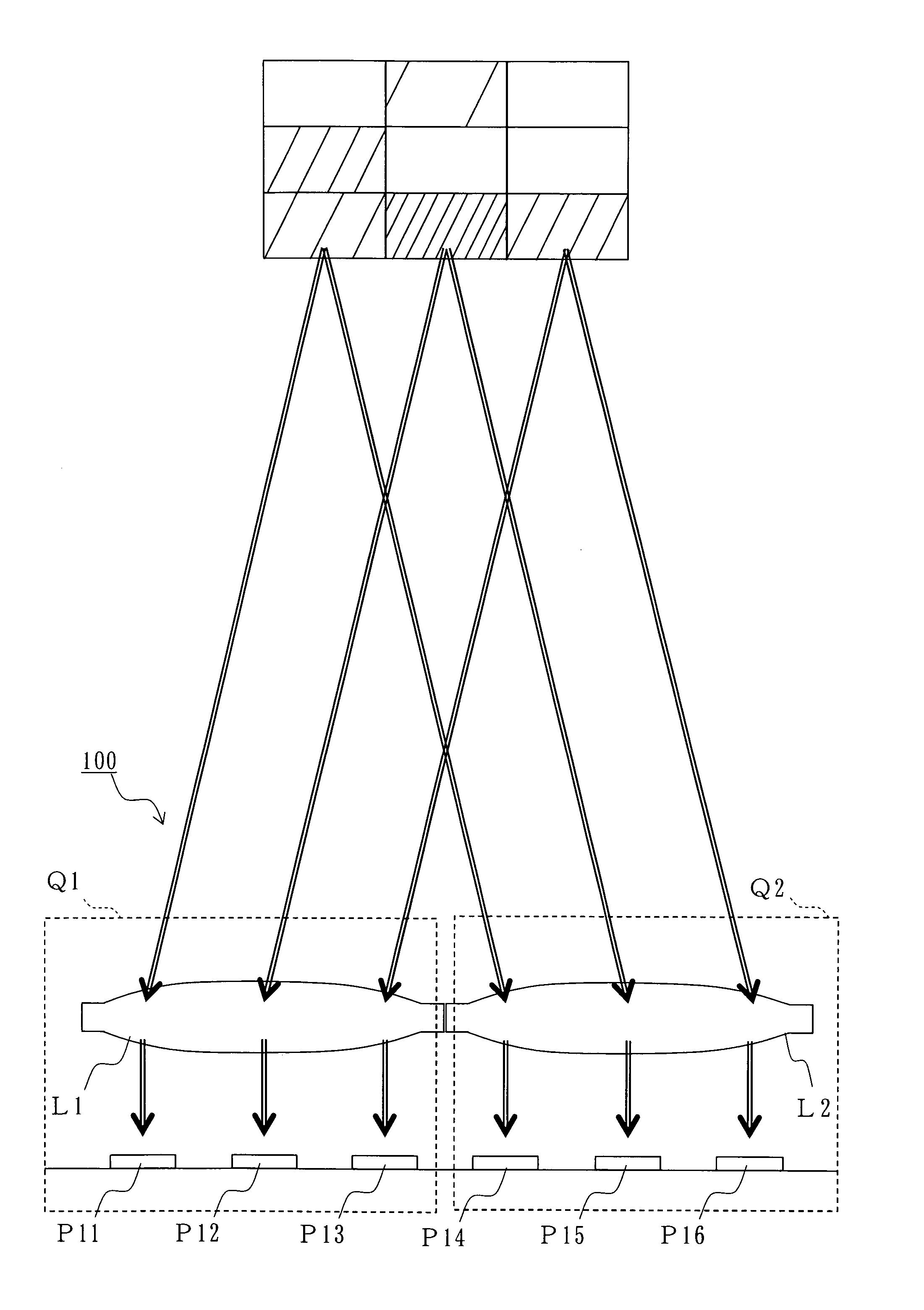
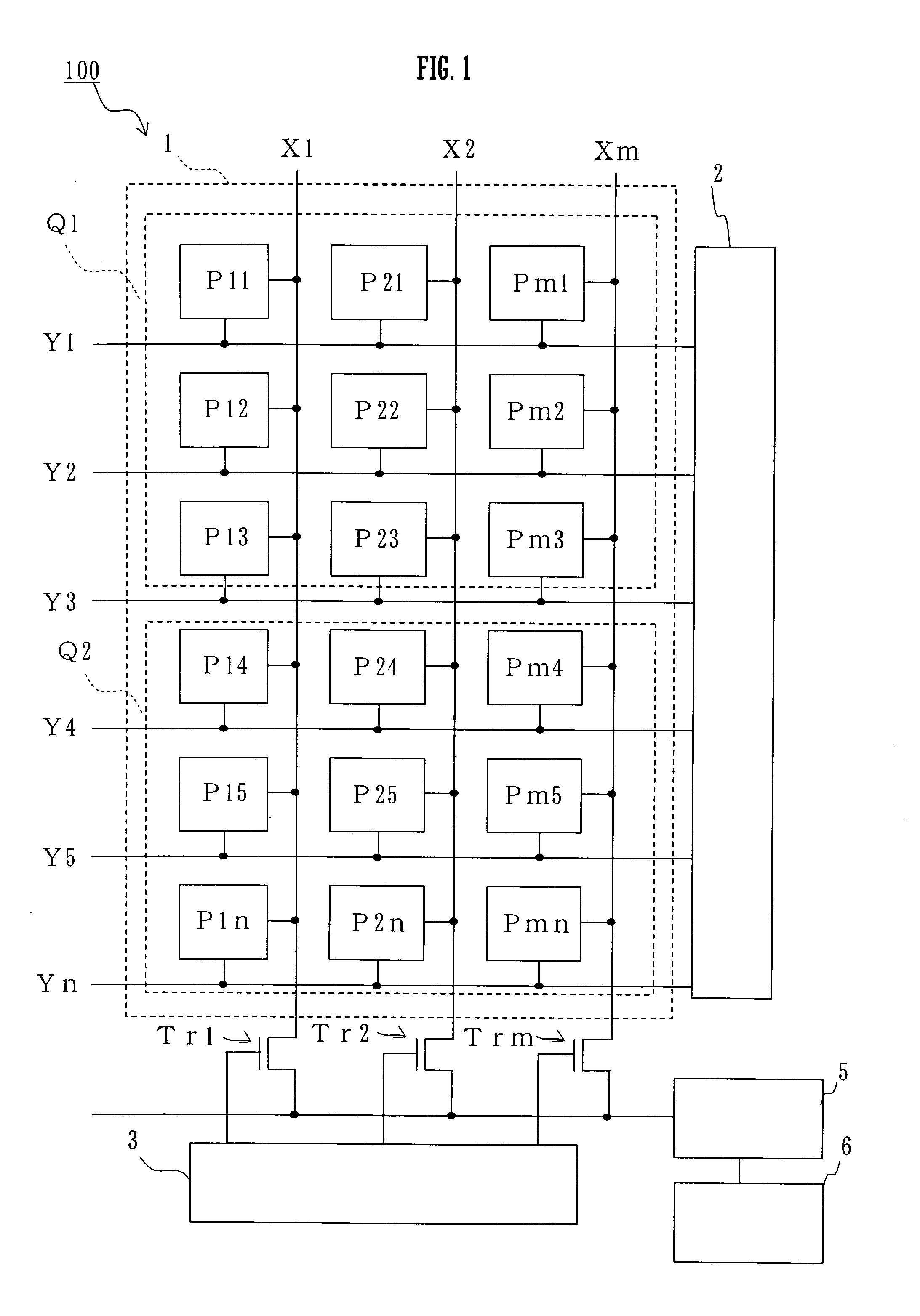
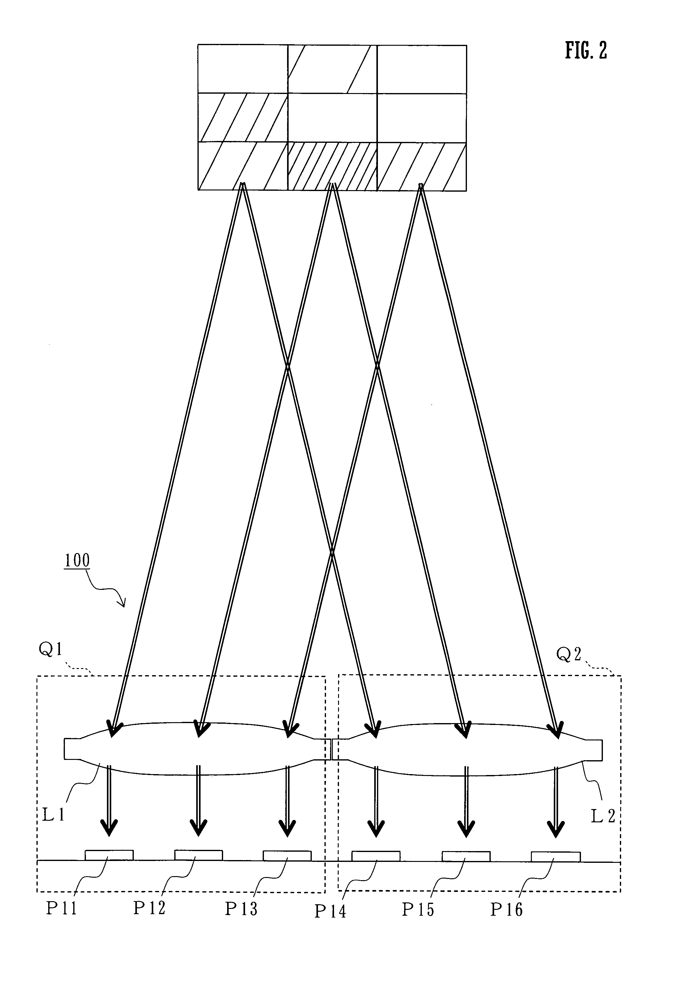
[0014] An embodiment of the present invention will now be explained. FIG. 1 is a block diagram showing a portion of the structure of a photographic device according to this embodiment. FIG. 2 is a conceptual figure for explanation of the focal point positions of certain elements in the optical system of this embodiment. And FIG. 3 is a conceptual figure for explanation of moving body detection processing by this embodiment.

[0015] The photographic device 100 shown in FIG. 1 comprises an image sensor 1 in which a plurality of pixels P11˜Pmn (m and n are positive integers) are arranged in the form of a matrix. This image sensor 1 faces an object to be photographed, via optical system elements not shown in the figure.

[0016] It should be understood that although here, for the convenience of illustration, an image sensor 1 with a reduced number of pixels is explained, in actual practice it is preferred for it to have several tens of thousands of pixels or more. Furthermore, although act...


PUM


Abstract

A photographic device includes an image sensor in which a plurality of pixels are arrayed. A horizontal scan circuit selects in order vertical drive lines to which the pixels are connected. And a vertical scan circuit reads voltages, due to accumulated electric charges, from the pixels in the horizontal row which is selected. A plurality of lenses are provided to the image sensor, arranged along the direction parallel to the vertical drive lines. Each of these lenses images an image of the same photographic region upon a pixel region which it confronts. The accumulated electric charges are read out from each pixel, arrayed in order. An image processing unit acquires a plurality of images of the photographic region spaced apart in time. And a moving body detection unit performs moving body detection from the differences between this plurality of images of the photographic region.

Description

CROSS REFERENCE [0001] This Nonprovisional application claims priority under 35 U.S.C. § 119(a) on Patent Application No. 2005-364575 filed in Japan on Dec. 19, 2005, the entire contents of which are hereby incorporated by reference.BACKGROUND OF THE INVENTION [0002] The present invention relates to a photographic device which photographs an image of a photographic region using an image sensor such as a CMOS image sensor or the like. [0003] A prior art photographic device which performs detection of a moving body from a plurality of images is per se known. The photographic device disclosed in Japanese Laid-Open Patent Publication Heisei 08-106534 photographs a plurality of images of the same photographic region at predetermined time steps. This device performs moving body detection from the differential between a plurality of images. [0004] With the device described above, in order to take a plurality of photographs of the same photographic region, it is necessary to perform photogr...

Claims


Application Information

Patent Timeline
Patent Type & Authority Applications(United States)
IPC IPC(8): H04N5/225G06V10/20H04N5/232H04N5/335H04N5/341H04N5/345H04N5/369H04N5/374H04N5/376
CPCG06T2200/28H04N5/144G06T7/254G06V10/20H04N25/41H04N25/531H04N25/76H04N25/00H04N25/48
Inventor NAKAO, YOSHIZUMITOYODA, TAKASHIMASAKI, YASUO
Owner FUNAI ELECTRIC CO LTD
Why Eureka
Try Eureka