Electronic circuit device and manufacturing method of the same

a technology of electronic circuit device and manufacturing method, which is applied in the direction of manufacturing tools, printed circuit non-printed electric components association, electric apparatus casing/cabinet/drawer, etc., can solve the problem that the holding pin provided in the molding die of a conventional electronic circuit device is unnecessary, and achieve the effect of reducing the cost of the molding die and improving the appearance of the molded casing

Active Publication Date: 2007-07-12
DENSO CORP
View PDF13 Cites 22 Cited by
  • Summary
  • Abstract
  • Description
  • Claims
  • Application Information

AI Technical Summary

Benefits of technology

[0007] It is an object of the present invention to provide an electronic circuit device and a manufacturing method of the same capable of preventing problems such as deformation of a circuit board or damage to electronic parts in a structure in which a case is molded to seal the circuit board with a resin material, while improving appearance of the molded case.
[0010] Since the circuit board is held to closely contact the molding die in the cavity of the molding die, a holding pin provided in a case molding die of a conventional electronic circuit device is unnecessary. Thus, a hole in the case is eliminated and an electronic circuit device having a casing with excellent appearance is provided. As a result, an electronic circuit device capable of preventing problems such as deformation of the circuit board or damage to the electronic parts while improving the appearance of the molded casing is realized.
[0013] The circuit board is held in the cavity of the molding die such that the circuit board closely contacts the molding die. Therefore, the holding pin of the case molding die of the conventional electronic circuit device is unnecessary. Thus, the cost of the molding die can be reduced. The hole formed in the case of the conventional electronic circuit device can be eliminated. Thus, the appearance of the molded casing can be improved.

Problems solved by technology

Since the circuit board is held to closely contact the molding die in the cavity of the molding die, a holding pin provided in a case molding die of a conventional electronic circuit device is unnecessary.

Method used


Image

  • Electronic circuit device and manufacturing method of the same
  • Electronic circuit device and manufacturing method of the same
  • Electronic circuit device and manufacturing method of the same

Examples


Embodiment Construction

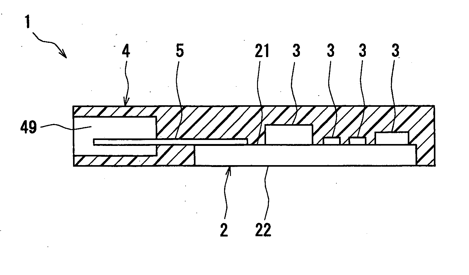
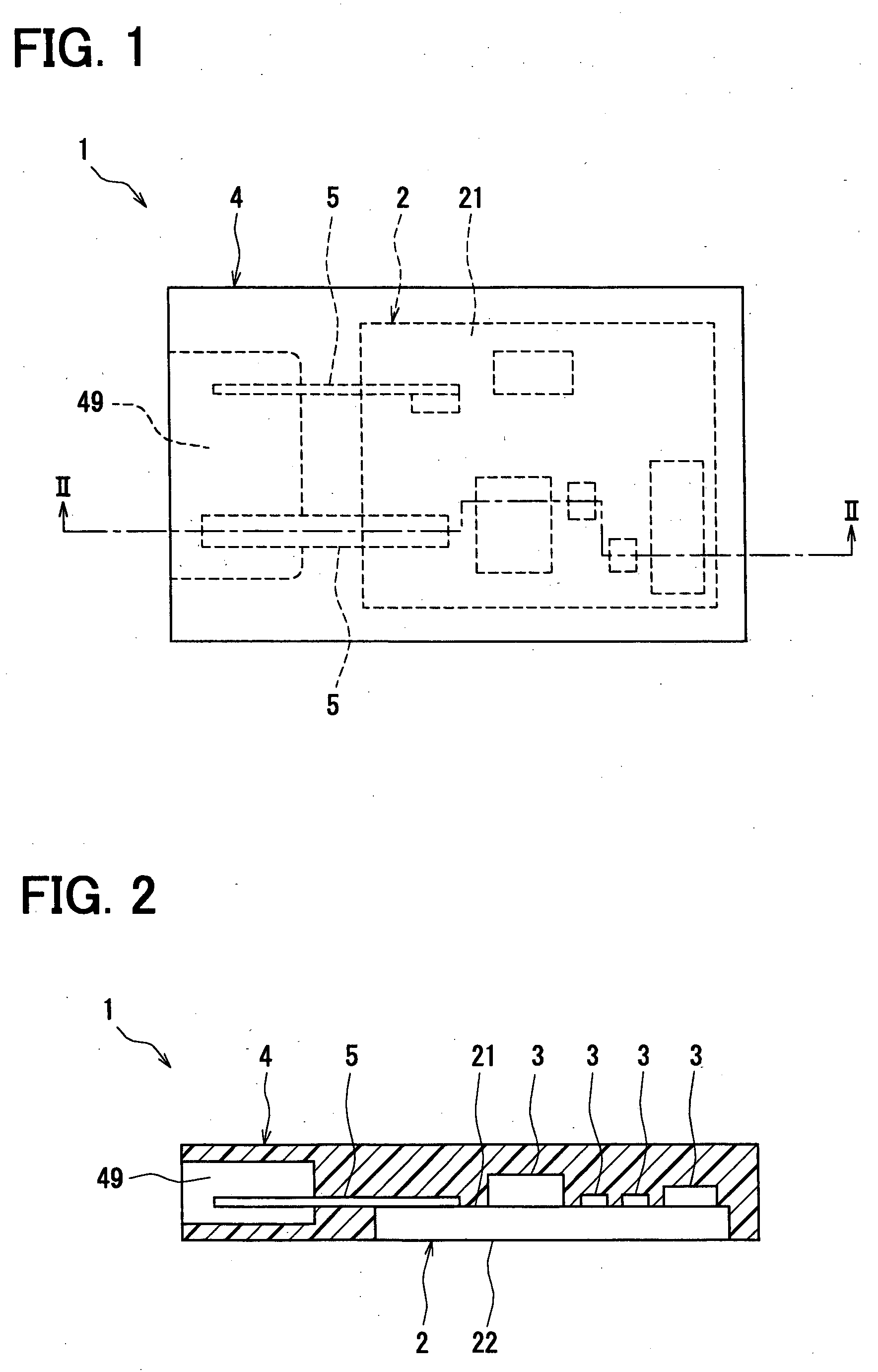
[0018] Referring to FIGS. 1 and 2, an electronic circuit device according to an example embodiment of the present invention is illustrated. As an example, the electronic circuit device according to the present embodiment is applied to an electronic key transmitting and receiving apparatus 1 as a transmitting and receiving apparatus of an electronic key system of an automobile and the like.

[0019] The electronic key transmitting and receiving apparatus 1 has a circuit board (printed board) 2 mounted with electronic parts 3, battery terminals 5 soldered to the circuit board 2, a casing 4 formed of a resin material to seal entire bodies of the electronic parts 3, the circuit board 2, and parts of the terminals 5, and the like as shown in FIGS. 1 and 2. A battery accommodation chamber 49 is formed in the casing 4. A battery and a battery cover are not shown in FIGS. 1 and 2.

[0020] The printed board 2 is made by forming a wiring pattern (not shown) of an electric conductor such as a cop...


PUM

PropertyMeasurementUnit
temperatureaaaaaaaaaa
melting pointaaaaaaaaaa
pressureaaaaaaaaaa

Abstract

A casing of an electronic key transmitting and receiving apparatus is formed to seal entire bodies of circuit parts, a mounting face of a printed board, on which the circuit parts are mounted, and parts of terminals while the other parts of the terminals are exposed. A rear face of the printed board opposite from the mounting face provides a part of an outer surface of the casing. When the printed board is provided in the casing through an insert molding process, the printed board is held in a cavity of a molding die such that the rear face of the printed board closely contacts an inner face of the cavity. Accordingly, deformation of the printed board due to pressure caused when the resin is poured or when the resin hardens is inhibited.

Description

CROSS REFERENCE TO RELATED APPLICATION [0001] This application is a divisional of U.S. application Ser. No. 11 / 408,076 filed Apr. 21, 2006 and is based on and incorporates herein by reference Japanese Patent Application No. 2005-125573 filed on Apr. 22, 2005.BACKGROUND OF THE INVENTION [0002] 1. Field of the Invention [0003] The present invention relates to an electronic circuit device and a manufacturing method of the same. For example, the present invention is suitably used in a transmitting and receiving apparatus of an electronic key system of an automobile and the like and a manufacturing method of the same. [0004] 2. Description of Related Art [0005] A known electronic circuit device as a transmitting and receiving apparatus of an electronic key system used in an automobile and the like accommodates a circuit board mounted with electronic parts, a battery and the like in a case in the shape of a flat plate (as described in JP-A-2004-52471, for example). [0006] Generally, the c...

Claims


Application Information

Patent Timeline
Patent Type & Authority Applications(United States)
IPC IPC(8): H05K1/00
CPCB29C45/14065B29C45/14639H05K3/284H05K2203/1316H05K5/065H05K2201/09754H05K2201/1034H05K3/3405H05K5/0034H05K1/18
Inventor SUGIMOTO, KEIICHINAKAGAWA, MITSURU
Owner DENSO CORP
Why Eureka
Try Eureka