Optical-element integrated semiconductor integrated circuit and fabrication method thereof

Inactive Publication Date: 2007-07-19
NEC CORP
View PDF1 Cites 6 Cited by
  • Summary
  • Abstract
  • Description
  • Claims
  • Application Information

AI Technical Summary

Benefits of technology

[0017] By means of the optical-element integrated LSI and the fabrication method of the LSI described in the foregoing explanation, the following effects can be obtained. Specifically, even when there is a plurality of input / output ports on an LSI and these input / output ports are further arranged irregularly at various positions, an optical-element integrated LSI can be provided in which photodetectors are mounted at the same height on each input port and light-emitting devices are mounted at the same height on each output port. By optically coupling with a plurality of optical circuits such as optical fiber and optical waveguides, this optical-element integrated LSI can realize high-speed, long-distance transmission that further features excellent resistance to noise. By matching the heights of coupling portions of optical circuits that the photodetectors are to optically join under the above-described conditions of use, the present invention can further obtain the effect of realizing highly efficient optical coupling for all channels of the optical elements. Still further, because the realization of highly efficient optical coupling on all channels enables effective use of the strength of optical signals, the present invention can further obtain the effect of further increasing the distance over which transmission can be realized. Alternatively, even when optical transmission is over short distances, the highly efficient optical coupling enables transmission of optical signals at higher strength, whereby the present invention can obtain the effect of improving resistance to noise.
[0018] In addition, because a plurality of optical elements are collectively mounted in batches, a decrease in the number of fabrication steps and a consequent decrease in cost can be anticipated compared to a case of successively mounting a plurality of optical elements one at a time. This effect becomes more conspicuous as the number of mounted optical elements increases.

Problems solved by technology

Although the processing speed of LSI is advancing toward ever-higher levels, there is a limit to the transmission capabilities of electrical wiring between a plurality of LSI, and attention has therefore focused on transmission that employs optical signals, which is not only capable of high-speed transmission and long-distance transmission but also features superior resistance to electromagnetic noise.
However, mounting a plurality of optical elements one at a time results in disparity in the heights of the photoreceptor surface and in light-emitting surface of each optical element and increased loss in optical coupling with external devices.
In addition, the mounting of optical elements becomes time-consuming and is prone to high costs.

Method used


Image

  • Optical-element integrated semiconductor integrated circuit and fabrication method thereof
  • Optical-element integrated semiconductor integrated circuit and fabrication method thereof
  • Optical-element integrated semiconductor integrated circuit and fabrication method thereof

Examples


first embodiment

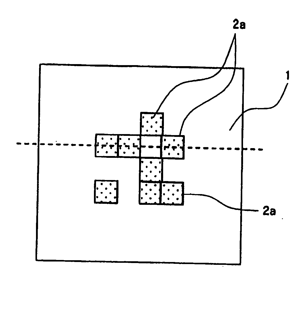
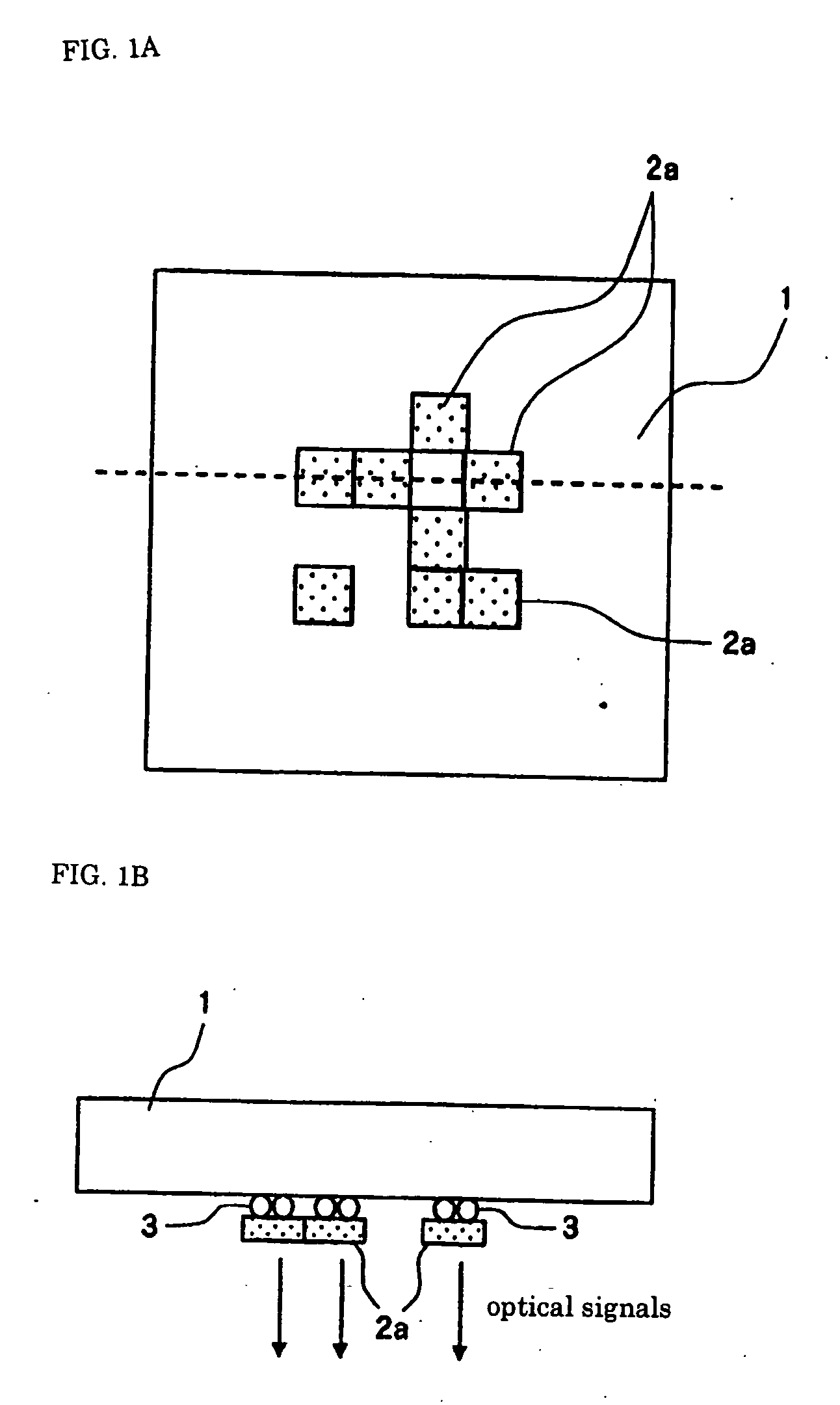
[0088] Explanation next regards the details of an example of an optical element integrated semiconductor integrated circuit (hereinbelow referred to as “optical-element integrated LSI”) of the present invention with reference to the figures. FIG. 1A is a schematic plan view showing the basic configuration of the optical-element integrated LSI of the present example, and FIG. 1B is a schematic sectional view. In the optical-element integrated LSI of this example, light-emitting device 2a is electrically connected by solder bumps 3 to electrical signal output ports (not shown) of LSI 1. There is a plurality of electrical signal output ports, and these electrical signal output ports are randomly arranged at various positions. In addition, light-emitting devices 2a are mounted at each electrical signal output port. Devices are used for light-emitting devices 2a that are capable of supplying light toward the rear-surface side (the downward side in FIG. 1B) of LSI 1. Accordingly, when an ...

second embodiment

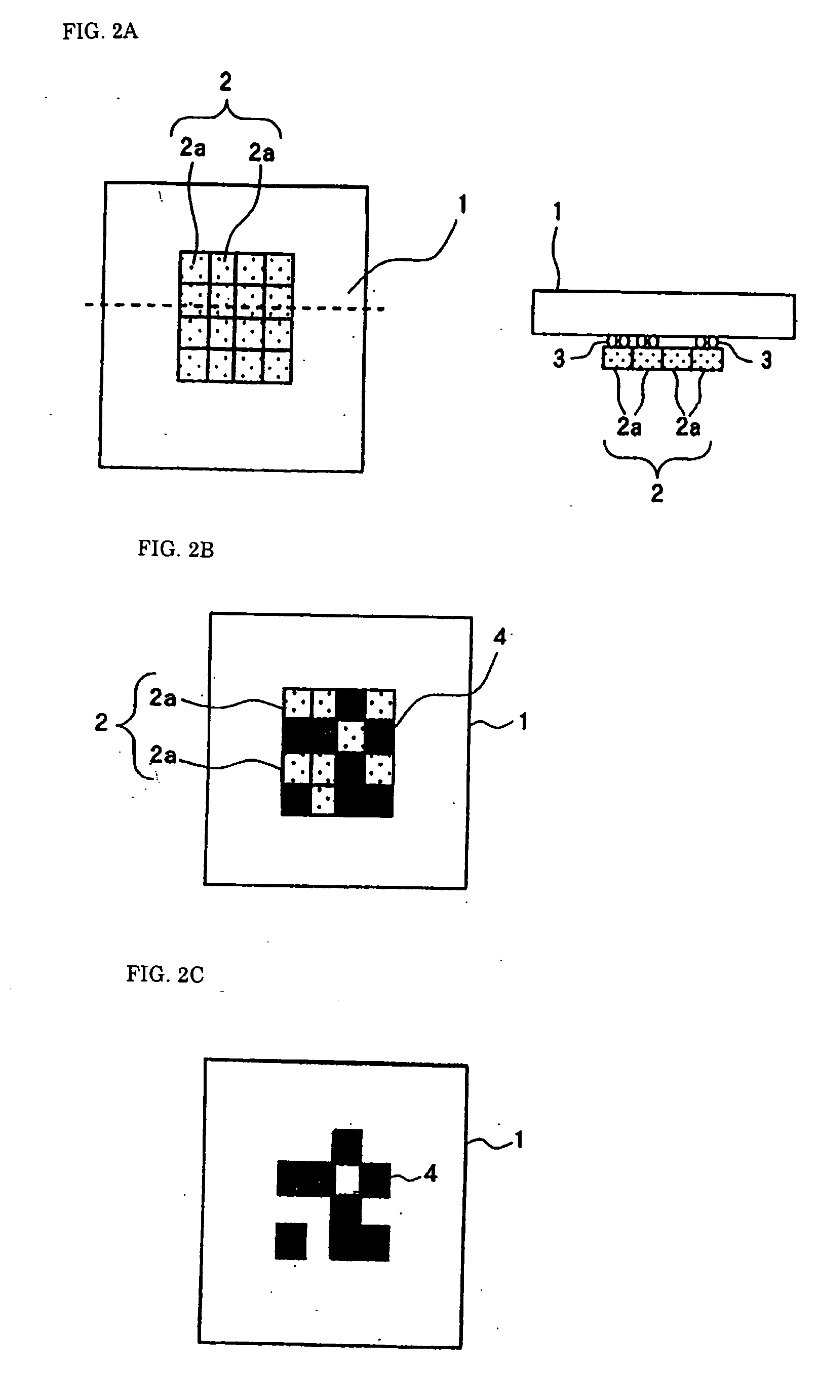
[0094] Explanation next regards the details of another example of an optical-element integrated LSI of the present invention with reference to the figures. FIG. 3 is a schematic plan view showing the general configuration of the optical-element integrated LSI of the present embodiment, and FIG. 3B is a schematic sectional view. In the optical-element integrated LSI of the present embodiment, photodetectors 5a are electrically connected by solder bumps 3 to electrical signal input ports (not shown) of LSI 1. There is a plurality of the above-described electrical signal input ports, and these electrical signal input ports are randomly arranged at various positions. In addition, photodetectors 5a are mounted on respective electrical signal input ports. Devices that can receive light that is incident from the rear surface (the lower side in FIG. 3B) of LSI 1 are used for photodetectors 5a. Accordingly, when ON / OFF optical signals are received as input from the outside, these optical sig...

third embodiment

[0100] Explanation next regards the details of another example of an optical-element integrated LSI of the present invention with reference to the figures. FIG. 5A is a schematic plan view showing the general configuration of the optical-element integrated LSI of the present embodiment, and FIG. 5B shows a schematic sectional view. In the optical-element integrated LSI of the present embodiment, light-emitting devices 2a are electrically connected by solder bumps 3 to electrical signal output ports (not shown) of LSI 1, and photodetectors 5a are electrically connected by solder bumps 3 to electrical signal input ports (not shown). LSI 1 has a plurality of electrical signal output ports and electrical signal input ports, and these ports are randomly arranged at various positions.

[0101] Devices capable of supplying light toward the rear-surface side (the downward side in FIG. 5B) of LSI 1 are used for light-emitting devices 2a. Thus, when an ON / OFF electrical signal is supplied as ou...


PUM


Abstract

Light-emitting device array 2 is mounted on LSI 1, following which necessary light-emitting devices 2a among two or more light-emitting devices 2 that make up mounted light-emitting device array 2 are allowed to remain and unnecessary light-emitting devices 2a are removed in order to mount light-emitting devices on a plurality of output ports that are randomly arranged on LSI 1.

Description

TECHNICAL FIELD [0001] The present invention relates to a semiconductor integrated circuit (hereinbelow also referred to as an “LSI”) and to a method of fabricating the semiconductor integrated circuit. BACKGROUND ART [0002] Although the processing speed of LSI is advancing toward ever-higher levels, there is a limit to the transmission capabilities of electrical wiring between a plurality of LSI, and attention has therefore focused on transmission that employs optical signals, which is not only capable of high-speed transmission and long-distance transmission but also features superior resistance to electromagnetic noise. It is believed that if an electrical signal that is supplied as output from a particular LSI is converted to an optical signal for transmission by an optical line and then reconverted to an electrical signal before input to another LSI, higher transmission speed can be realized than when using an electrical signal alone. [0003] JP-A-2001-036197 discloses an optoel...

Claims


Application Information

Patent Timeline
IPC IPC(8): H01L33/00H01L31/12H01L29/207H01L27/15H01L29/26H01L25/16H01L27/14H01L33/48H01L33/58H01L33/60H01L33/62
CPCH01L31/12H01L25/167H01L2924/0002H01L2924/00
Inventor ODA, MIKIOTAKAHASHI, HISAYANAKANO, KAICHIROKOUTA, HIKARUKOBAYASHI, KOHROH
Owner NEC CORP
Why Eureka
Try Eureka