High hysteresis width input circuit

Inactive Publication Date: 2005-09-29
SEIKO EPSON CORP
View PDF1 Cites 0 Cited by
  • Summary
  • Abstract
  • Description
  • Claims
  • Application Information

AI Technical Summary

Benefits of technology

[0044] Furthermore, providing the first input circuit including the N-type MOSFET and the second input circuit including the P-type MOSFET makes it possible to set two logic levels independently of each other, which increases the degree of freedom in setting the conductance constant ratio, makes the design easier and can increase the hysteresis width as well.
[0055] As shown above, the present invention has the effect of reliably providing a hysteresis input circuit having a large hysteresis width, resistant to noise even when the supply voltage (operating voltage) becomes a low voltage.

Problems solved by technology

However, with the introduction of finer integrated circuits and reduction of withstand voltages, lower supply voltages are used in recent years and it is becoming impossible to secure a sufficient hysteresis width.
However, the above described conventional hysteresis input circuits have the following problems.
However, it is actually impossible to set the conductance constant ratio (βN / βP) to 0 or infinity, and therefore the hysteresis width is actually much smaller than this value.
Therefore, when the supply voltage VDD is a low voltage, for example, approximately 1.5 V, since VTP or VTN is approximately 0.5 V to 0.7 V, the hysteresis width becomes very small and cannot accomplish the original objective.
Therefore, as the conventional circuits shown in FIG. 7, FIG. 8 and FIG. 9, the hysteresis input circuit whose equivalent circuit can be reduced to an inverter circuit has a problem that it is not possible to take a sufficient hysteresis width at a low voltage.
Furthermore, during a low-voltage operation, too, if an attempt is made to set a conductance constant ratio (βN / βP) to secure the hysteresis width as much as possible, it is necessary to change the forms of P-type MOSFETs or N-type MOSFETs to an unnatural extent, resulting in problems of occupying a large chip area, reducing driving capacity or deteriorating responsivity.
However, under a design condition under which the hysteresis width should be secured, the first logic level is in effect determined by the N-type MOSFET 912 and P-type MOSFET 915, which results in the following problem.
However, such a setting is a setting between the P-type MOSFET and N-type MOSFET which differ in nature, and therefore it is rather hard to extend the hysteresis to the very limit when a variation in manufacturing is also taken into consideration.
Furthermore, as is also understandable from Expression (8), even if the logic level VIL is forcibly set low and the logic level VIL falls below potential 0 due to a variation in volume production, there is a problem that even if the potential of an input signal of the input terminal 920 is changed within a range of the supply voltage, a latched state may continue and it may be impossible to recover the operation.
Also when the first logic level VIH is set, a forcible setting to secure the hysteresis width causes the logic level VIH to exceed the supply voltage VDD, causes a latched state to continue, making it impossible to recover the operation.

Method used


Image

  • High hysteresis width input circuit
  • High hysteresis width input circuit
  • High hysteresis width input circuit

Examples


embodiment 1

(Embodiment 1)

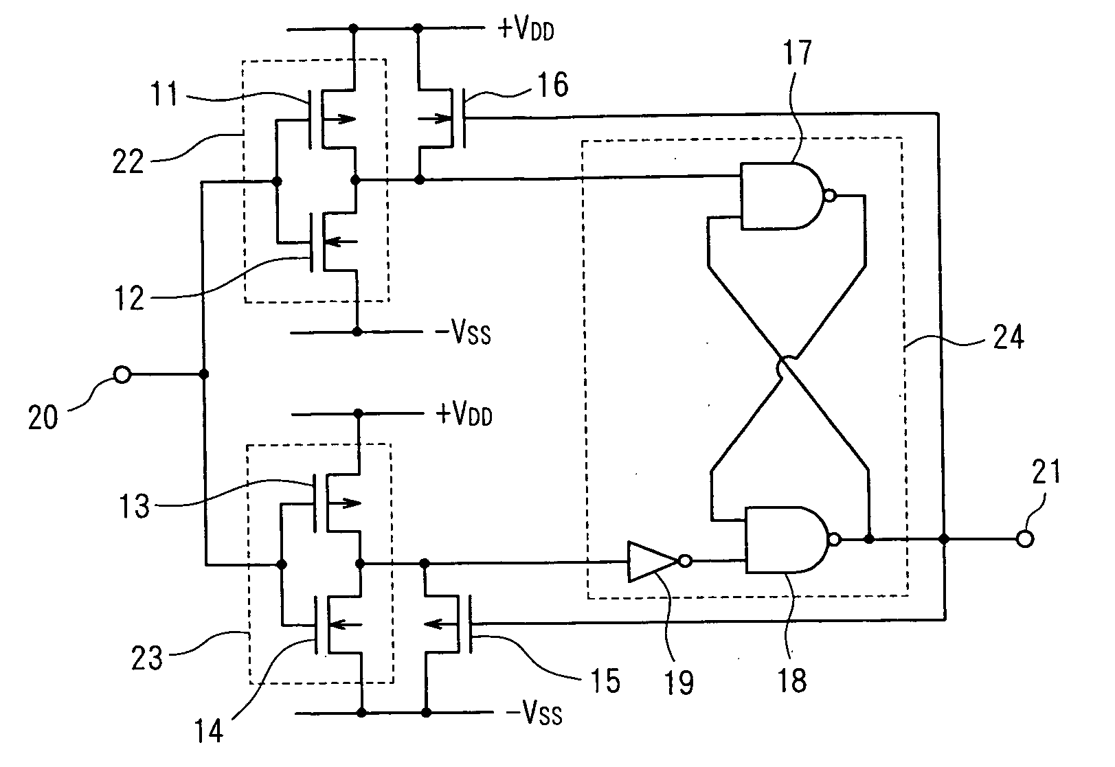
[0067]FIG. 1 is a circuit diagram showing a first embodiment of the present invention.

[0068] As shown in FIG. 1, this first embodiment is provided with an inverter circuit 22, an inverter circuit 23, a latch circuit 24, an N-type MOSFET 16 and a P-type MOSFET 15 and these are formed into an integrated circuit.

[0069] The inverter circuit 22 is made up of a CMOS inverter circuit which combines a P-type MOSFET 11 and an N-type MOSFET 12 and operates on a power supply +VDD of a positive electrode and a power supply −VSS of a negative electrode.

[0070] That is, the source electrode of the P-type MOSFET 11 is connected to the power supply +VDD of the positive electrode. The source electrode of the N-type MOSFET 12 is connected to the power supply −VSS of the negative electrode. The gate electrodes of the P-type MOSFET 11 and the N-type MOSFET 12 are connected together and their common connection section is connected to an input terminal 20. Furthermore, the drain electrode...

modification example of embodiment 1

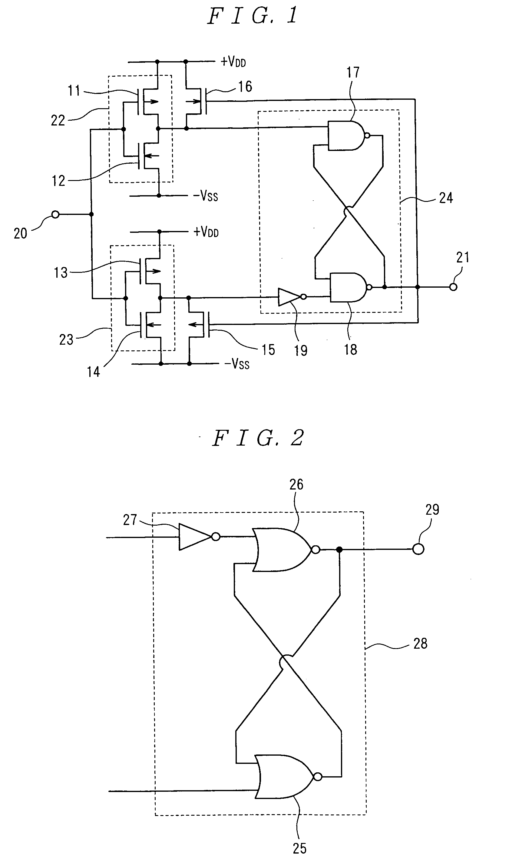
[0123] The present invention is not limited to the first embodiment shown in FIG. 1. FIG. 1 shows an example of the latch circuit 24 made up of NAND circuits 17, 18 and an inverter circuit 15, but this is only an example and this latch circuit can be replaced by a latch circuit 28 made up of NOR circuits 25, 26 and inverter circuit 27 as shown in FIG. 2.

[0124] In this case, however, the output of the inverter circuit 22 in FIG. 1 is connected to the input of the inverter circuit 27 in FIG. 2 and the output of the inverter circuit 23 in FIG. 1 is connected to the first gate of the NOR circuit 25 in FIG. 2.

[0125] Furthermore, regarding the setting of (βNS / βN1) of conditional Expression (16) and (βPS / βP1) of conditional Expression (29), the setting method by changing the channel width of a MOSFET transistor has been explained, but it is also possible to use a method of changing a channel length of a transistor. When the channel width is increased, β is increased, but when the channel...

embodiment 2

[0128]FIG. 4 is a circuit diagram showing a second embodiment of the present invention.

[0129] As shown in FIG. 4, this second embodiment is provided with an inverter circuit 42, a buffer circuit 43, an N-type MOSFET 33 and a P-type MOSFET 34 and these are formed into an integrated circuit.

[0130] The inverter circuit 42 is made up of a CMOS inverter circuit combining a P-type MOSFET 31 and an N-type MOSFET 32 and operates on a power supply +VDD of a positive electrode and a power supply −VSS of a negative electrode.

[0131] That is, the source electrode of the P-type MOSFET 31 is connected to the power supply +VDD of the positive electrode. The source electrode of the N-type MOSFET 32 is connected to the power supply −VSS of the negative electrode. Furthermore, both gate electrodes of the P-type MOSFET 31 and N-type MOSFET 32 are connected together and a common connection section is connected to an input terminal 40. Furthermore, the drain electrodes of the P-type MOSFET 31 and N-ty...


PUM


Abstract

The present invention is constructed of a first input circuit having a higher logic level VIH made up of a first inverter circuit 22 controlled by an input signal and an N-type MOSFET 16 controlled by a latch circuit 24 which stores a preceding state, a second input circuit having a lower logic level VIL made up of a second inverter circuit 23 controlled by an input signal and a P-type MOSFET 15 controlled by a latch circuit which stores a preceding state and the latch circuit 24 which stores a preceding state.

Description

BACKGROUND OF THE INVENTION [0001] 1. Field of the Invention [0002] The present invention relates to a semiconductor integrated circuit using an insulated gate field-effect transistor (hereinafter referred to as “MOSFET”), and more particularly, to a hysteresis input circuit whose logic level is provided with a hysteresis characteristic to eliminate misoperation or instability due to noise when an input signal of an input circuit is changed from a high potential to a low potential or from a low potential to a high potential, capable of securing a large enough hysteresis width even when a supply voltage decreases. [0003] 2. Description of the Related Art [0004] Conventionally, for an integrated circuit, a digital circuit in particular, a hysteresis input circuit is widely used with an input signal terminal provided with a difference in the logic level between a rise and fall of an input signal, that is, a hysteresis characteristic so as to eliminate misoperation or instability due to...

Claims


Application Information

Patent Timeline
IPC IPC(8): H03K3/037H03K3/3565
CPCH03K3/3565H03K3/0377
Inventor HASHIMOTO, MASAMI
Owner SEIKO EPSON CORP
Why Eureka
Try Eureka