Semiconductor device using sige for substrate and method for fabricating the same

a technology of semiconductor devices and substrates, applied in the direction of semiconductor devices, electrical devices, transistors, etc., can solve the problems of hard mask on the gate electrode eroded and stripped away, source/drain and gate electrode also may be shorted, and it is difficult to recess into the source/drain region

Inactive Publication Date: 2007-07-19
KK TOSHIBA
View PDF99 Cites 36 Cited by
  • Summary
  • Abstract
  • Description
  • Claims
  • Application Information

AI Technical Summary

Benefits of technology

[0034]FIG. 9 is a cross-sectional view illustrating a fabrication step of a conventional MOS transistor;

Problems solved by technology

However, when the source / drain regions are being recessed, there may occur a case in which the hard mask on the gate electrode is eroded and stripped away by the source / drain recess.
Further, the source / drain and the gate electrode also may be shorted.
It is thus difficult to recess into the source / drain region deeply, i.e. the epitaxially grown SiGe layers, and it is hard to further enhance the performance of the MOS transistor.

Method used


Image

  • Semiconductor device using sige for substrate and method for fabricating the same
  • Semiconductor device using sige for substrate and method for fabricating the same
  • Semiconductor device using sige for substrate and method for fabricating the same

Examples


first embodiment

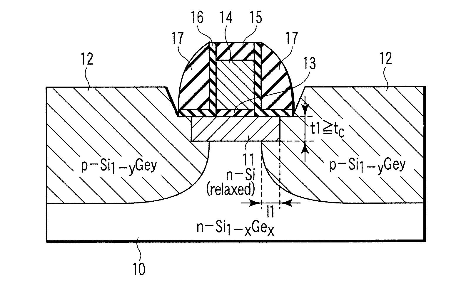
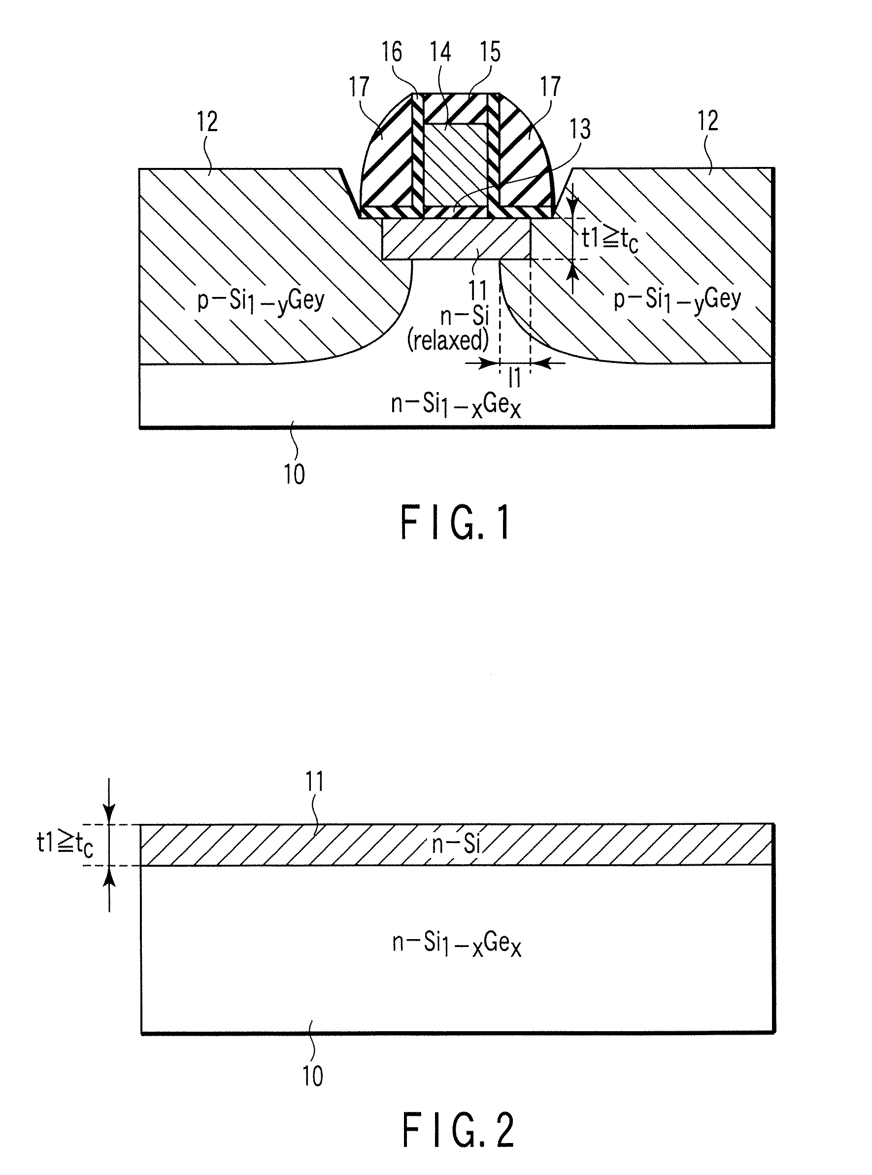
[0051] A semiconductor device according to the present invention and a method for fabricating the semiconductor device will now be described with reference to FIG. 1. FIG. 1 is a cross-sectional view of a p-channel MOS transistor according to this embodiment.

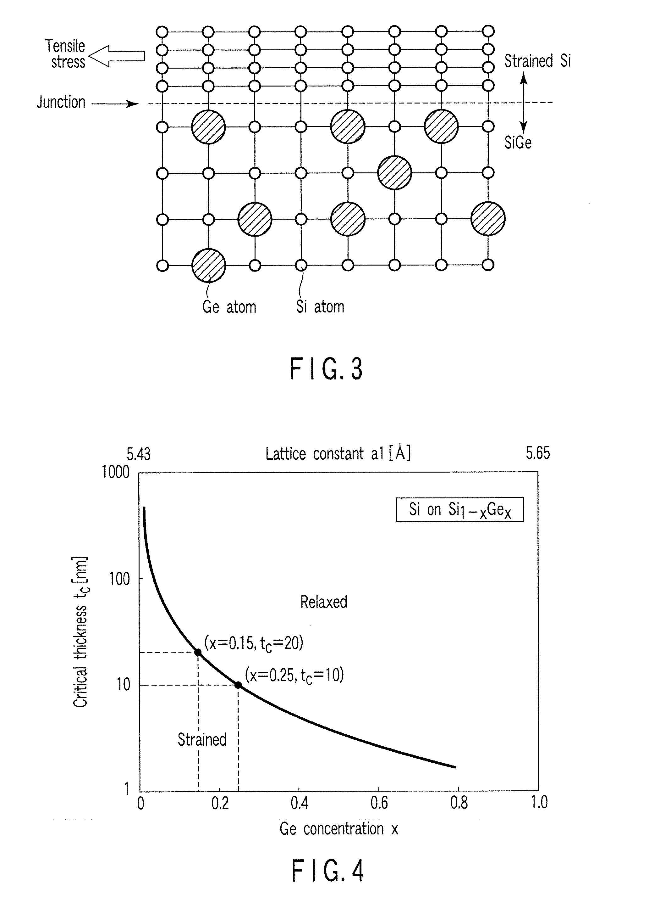
[0052] As shown in FIG. 1, an n-type Si layer 11 is formed on an n-type Si1-xGex (x=a positive number less than 1) layer 10. A film thickness t1 of the Si layer 11 is not less than a critical thickness tc relative to the Si1-xGex layer 10. The critical thickness, in this context, is such a film thickness that if the film thickness of the Si layer 11 is set at tc or more, no strain occurs due to a lattice mismatching with an underlayer of the Si layer 11 (i.e. strain is relaxed). In other words, if the film thickness of the Si layer 11 is set at less than tc, strain occurs due to the influence of the underlayer. The thickness of the Si layer 11 according to the present embodiment is set at the critical film thickness tc or more. ...

second embodiment

[0105]FIG. 23 is a cross-sectional view of a p-channel MOS transistor. As shown in FIG. 23, in the structure shown in FIG. 12 which has been described in connection with the second embodiment, an SiC layer 50 is substituted for the SiGe layer 10. In this case, an Si layer 52 may be substituted for the SiGe layer 12. In the present structure, SiC having a smaller lattice constant than Si is used for the substrate 50. Accordingly, the lattice constant of the Si layer 20, which is formed by using strained silicon, is less than that of Si. Hence, a compressive stress can be introduced to the Si layer 20 by using SiGe and Si for the source and drain.

[0106]FIG. 24 is a cross-sectional view of a p-channel MOS transistor. As shown in FIG. 24, in the structure shown in FIG. 1 which has been described in connection with the first embodiment, an SiC layer 50 may be substituted for the SiGe layer 10.

third embodiment

[0107]FIG. 25 is a cross-sectional view of an n-channel MOS transistor. As shown in FIG. 25, in the structure shown in FIG. 13 which has been described in connection with the third embodiment, an SiC layer 60 is substituted for the SiGe layer 30, an unstrained Si layer 61 (with a thickness not less than the critical thickness at which the stress due to lattice mismatching with SiC is relaxed) is substituted for the Si layer 31, and an SiC layer 62 is substituted for the SiGe layer 32. With this structure, a tensile stress can be introduced to the Si layer 61 by the SiC layer 62 having a smaller lattice constant than Si.

[0108] Not only the SiC, but also GaAs is usable as material. In addition, a ternary compound semiconductor or a quaternary compound semiconductor, which includes In, Al, etc. in addition to GaAs, is usable. Besides, the SiGe layer 10, 30, which serves as the substrate, may be formed, for example, on an insulating film that is formed on a silicon substrate (SGOI struc...


PUM


Abstract

A semiconductor device includes a first semiconductor layer, an n-type/p-type second semiconductor layer, p-type/n-type third semiconductor layers and a first gate electrode. The second semiconductor layer is formed on the first semiconductor layer and has an oxidation rate which is lower than that of the first semiconductor layer. The third semiconductor layers are formed in the second semiconductor layer and have a depth reaching an inner part of the first semiconductor layer. In case that the second and third semiconductor layers are n-type and p-type, respectively, a lattice constant of the second semiconductor layer is less than that of the third semiconductor layer. In case that the second and third semiconductor layers are p-type and n-type, respectively, the lattice constant of the second semiconductor layer is greater than that of the third semiconductor layer. A first gate electrode is formed on the second semiconductor layer.

Description

CROSS-REFERENCE TO RELATED APPLICATIONS [0001] This application is based upon and claims the benefit of priority from prior Japanese Patent Application No. 2006-001812, filed Jan. 6, 2006, the entire contents of which are incorporated herein by reference. BACKGROUND OF THE INVENTION [0002] 1. Field of the Invention [0003] The present invention relates generally to a semiconductor device and a method for fabricating the semiconductor device, and relates, for example, to a MOS transistor using SiGe for a substrate. [0004] 2. Description of the Related Art [0005] Conventionally, there is known a MOS transistor in which a source region and a drain region are formed by SiGe, as disclosed, for instance, in Jpn. Pat. Appln. KOKAI Publication No. 2005-142431. [0006] In this type of transistor, an epitaxial SiGe is grown on the recessed source / drain region while gate-electrode is covered with hard mask, e.g. SiN, so that SiGe will not grow on it. In this structure, as the depth of the recess...

Claims


Application Information

Patent Timeline
Patent Type & Authority Applications(United States)
IPC IPC(8): H01L29/94
CPCH01L21/823425H01L21/823807H01L21/823814H01L29/7848H01L29/165H01L29/66628H01L29/66636H01L29/1054
Inventor KAWASAKI, HIROHISA
Owner KK TOSHIBA
Why Eureka
Try Eureka