Semiconductor devices and methods of manufacture thereof

a technology of semiconductor devices and integrated circuits, applied in semiconductor devices, semiconductor/solid-state device details, electrical apparatus, etc., can solve the problems of difficult manufacturing of ics with multiple types of circuitry, low power consumption and increased speed, and difficulty in the etching process required to produce vertical connections between vertically stacked ics

Inactive Publication Date: 2007-07-19
INFINEON TECH AG
View PDF22 Cites 145 Cited by
  • Summary
  • Abstract
  • Description
  • Claims
  • Application Information

AI Technical Summary

Benefits of technology

[0009] These and other problems are generally solved or circumvented, and technical advantages are generally achieved, by preferred embodiments of the present invention, which provide novel methods of connecting two or more ICs together to form 3D-ICs and structures thereof.

Problems solved by technology

However, it can be difficult to manufacture an IC with multiple types of circuitry, due to integration problems of the different circuit fabrication technologies.
3D-ICs are predicted to be used in the future for low power, high speed applications, because the paths of conduction may be shortened by the vertical electrical connections between the circuits, resulting in low power consumption and increased speed.
However, 3D-ICs introduce some design and fabrication challenges.
For example, the etch processes required to produce the vertical connections between vertically stacked ICs may be difficult, due to the many different types of material layers and the thickness of the material layers that must be etched.

Method used


Image

  • Semiconductor devices and methods of manufacture thereof
  • Semiconductor devices and methods of manufacture thereof
  • Semiconductor devices and methods of manufacture thereof

Examples


Embodiment Construction

[0019] The making and using of the presently preferred embodiments are discussed in detail below. It should be appreciated, however, that the present invention provides many applicable inventive concepts that can be embodied in a wide variety of specific contexts. The specific embodiments discussed are merely illustrative of specific ways to make and use the invention, and do not limit the scope of the invention.

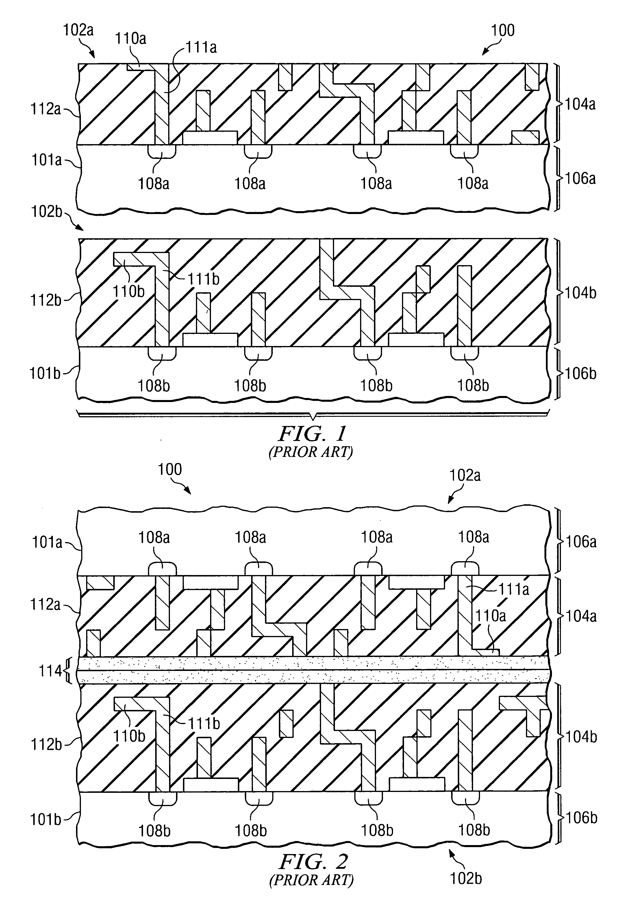
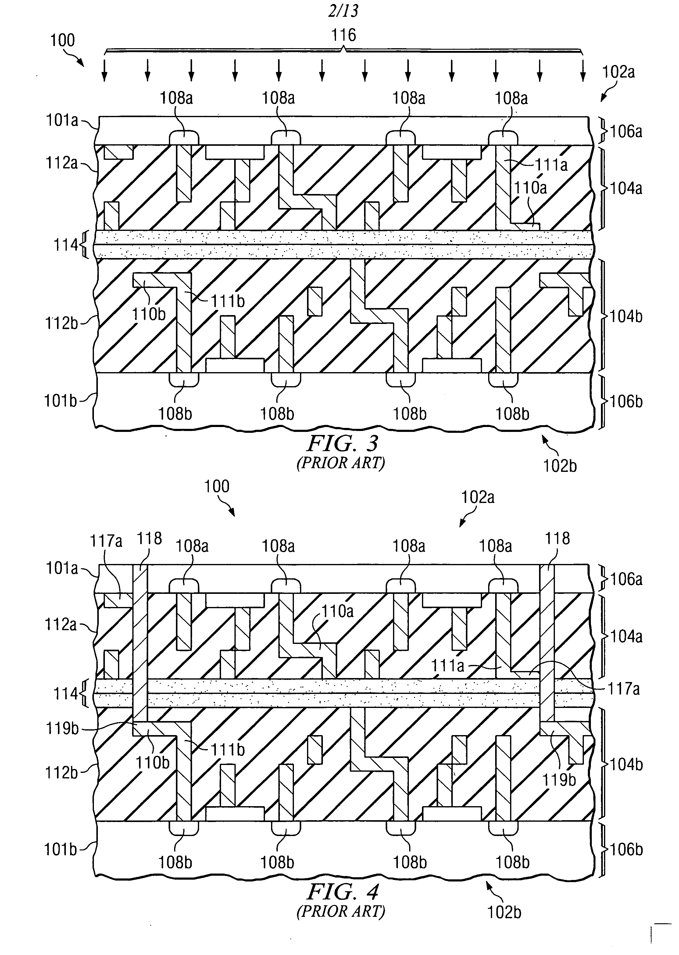
[0020]FIGS. 1 through 4 show cross-sectional views of a prior art method of fabricating a 3D-IC at various stages of manufacturing. Referring first to FIG. 1, two integrated circuits 102a and 102b are independently manufactured. For example, integrated circuit 102a comprises a workpiece 101a. Active areas 108a are formed within and over the workpiece 101a, as shown. The active areas 108a may include transistors, as shown, or the active areas 108a may comprise other devices or circuit components. The workpiece 101a and the active areas 108a are labeled 106a to indicate the p...


PUM


Abstract

Vertically stacked integrated circuits and methods of fabrication thereof are disclosed. Deep vias that provide vertical electrical connection for vertically stacked integrated circuits are formed early in the manufacturing process, before integrated circuits are bonded together to form a three dimensional integrated circuit (3D-IC).

Description

TECHNICAL FIELD [0001] The present invention relates generally to the fabrication of semiconductor devices, and more particularly to the fabrication of vertically stacked integrated circuits. BACKGROUND [0002] Semiconductor devices are used in a variety of electronic applications, such as computers, cellular phones, personal computing devices, and many other applications. Home, industrial, and automotive devices that in the past comprised only mechanical components now have electronic parts that require semiconductor devices, for example. [0003] Semiconductor devices are manufactured by depositing many different types of material layers over a semiconductor workpiece or wafer, and patterning the various material layers using lithography. The material layers typically comprise thin films of conductive, semiconductive, and insulating materials that are patterned and etched to form integrated circuits (ICs). There may be a plurality of transistors, memory devices, switches, conductive ...

Claims


Application Information

Patent Timeline
Patent Type & Authority Applications(United States)
IPC IPC(8): H01L21/00
CPCH01L21/76898H01L23/481H01L2924/1305H01L2924/1306H01L2224/80895H01L25/0657H01L25/50H01L2224/9202H01L2225/06513H01L2225/06541H01L2924/01057H01L2924/01078H01L2924/01019H01L2224/05548H01L2224/80357H01L24/80H01L2924/00H01L2924/14H01L2224/80896H01L2224/80986
Inventor KNORR, ANDREAS
Owner INFINEON TECH AG
Why Eureka
Try Eureka