Semiconductor device and method of manufacturing the same

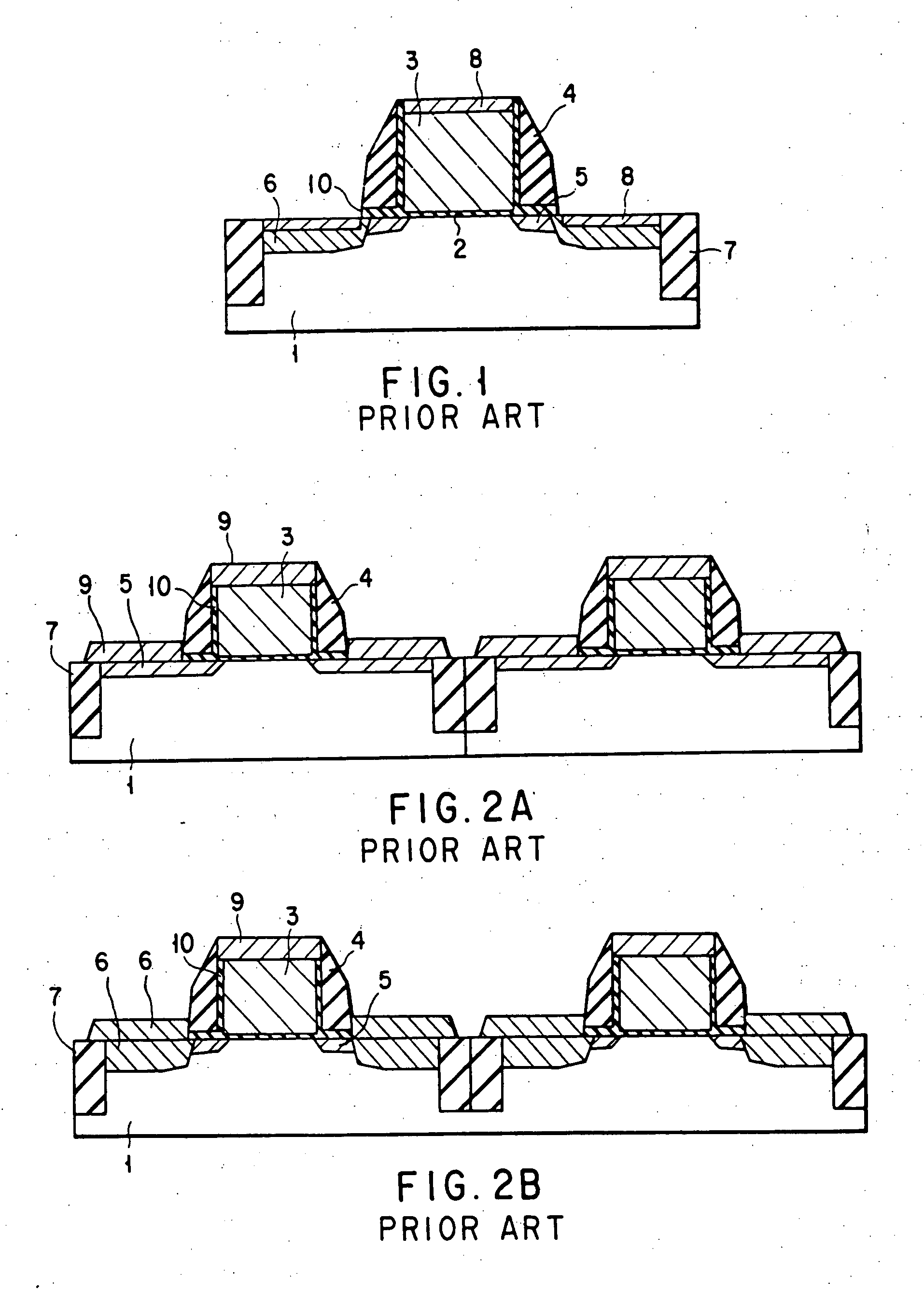
a semiconductor and semiconductor technology, applied in the direction of semiconductor devices, electrical devices, transistors, etc., can solve the problems of reducing the width of the gate electrode to about 0.1 m, the inability to complete ion implantation within an actual processing time, and the difficulty of maintaining an insulating state between adjacent transistors, so as to reduce the size and prevent punching

Inactive Publication Date: 2007-07-26
KK TOSHIBA
View PDF17 Cites 5 Cited by
  • Summary
  • Abstract
  • Description
  • Claims
  • Application Information

AI Technical Summary

Benefits of technology

[0013] It is an object of the present invention to provide a semiconductor device capable of reducing its size and preventing punch-through, and a method of manufacturing the same.
[0014] It is another object of the present invention to provide a semiconductor device capable of maintaining an insulating state between devices even upon a reduction in size, and a method of manufacturing the same.
[0015] It is still another object of the present invention to provide a semiconductor device capable of reducing its size, preventing punch-through, and maintaining an insulating state between devices, and a method of manufacturing the same.

Problems solved by technology

However, a reduction in gate electrode width to about 0.1 μm poses the following problems.
However, at a low acceleration voltage, the ion current decreases, so ion implantation cannot be complete within an actual processing time.
As a result, the Si film 9 is also formed on a device isolation region 7, making it difficult to maintain an insulating state between adjacent transistors.
Therefore, the above-described problems also occur in the pMOS.

Method used


Image

  • Semiconductor device and method of manufacturing the same
  • Semiconductor device and method of manufacturing the same
  • Semiconductor device and method of manufacturing the same

Examples


first embodiment

[0048] The first embodiment will be explained.

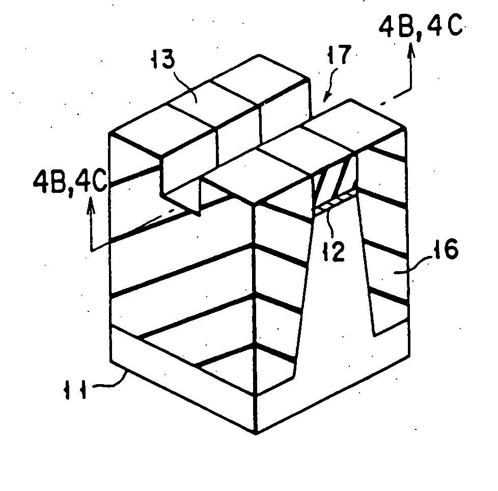
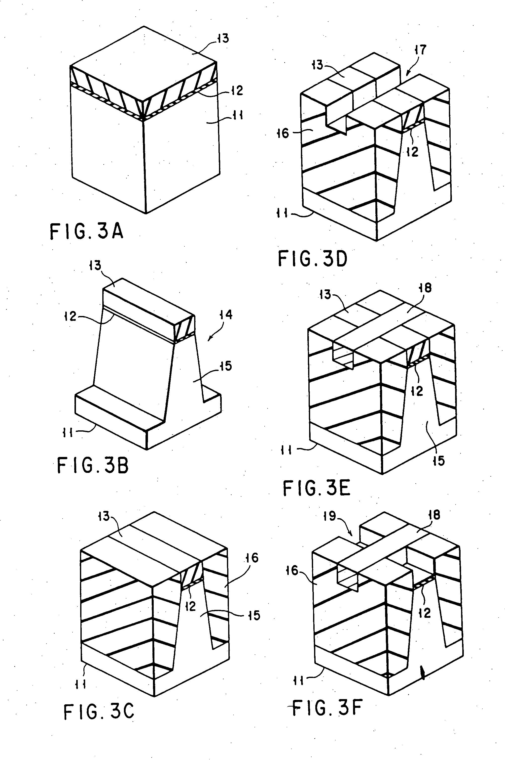
[0049]FIGS. 3A to 3K are perspective views, respectively, schematically showing the manufacturing steps according to the first embodiment of the present invention. The first embodiment will be described with reference to FIGS. 3A to 3K.

[0050] As shown in FIG. 3A, a thermal oxide film 12 having a thickness of about 5 nm is formed on an exposed (100) face of a silicon substrate 11. Silicon nitride is deposited by LPCVD on the thermal oxide film 12 to form a silicon nitride film 13 having a thickness of about 150 nm.

[0051] A resist pattern (not shown) is formed on the silicon nitride film 13 by photolithography or EB lithography. As shown in FIG. 3B, the silicon nitride film 13, the oxide film 12, and the silicon substrate 11 are etched by RIE (Reactive Ion Etching) to form a device region 15. A groove 14 formed at this time is used for device isolation (STI: Sallow Trench Isolation). The trench depth is set to about 300 nm.

[0052] Then, ...

second embodiment

[0070] the present invention will be described.

[0071]FIGS. 7A to 7D are sectional views, respectively, schematically showing the manufacturing steps according to the second embodiment of the present invention. Note that the steps in the second embodiment are the same as those in the first embodiment except for only the step shown in FIG. 3I. Only a step corresponding to the step shown in FIG. 3I is therefore explained.

[0072] In the second embodiment, as shown in FIG. 7A, a silicide film 22 does not completely fill a groove in the source / drain region. For this reason, the groove formed by the silicide film 22 is filled with a TEOS oxide film 41 by CVD, and its surface is flattened by CMP, as shown in FIG. 7B. If necessary, the silicide film 22 is recessed by about 50 nm after the step in FIG. 7B, as shown in FIG. 7C. The formed groove is filled with a TEOS oxide film 42 by CVD and flattened, as shown in FIG. 7D. Accordingly, cap films made of the TEOS oxide films 41 and 42 can be fo...

third embodiment

[0074] the present invention will be described.

[0075]FIGS. 8A to 8F are perspective views, respectively, schematically showing the manufacturing steps according to the third embodiment of the present invention. Note that the steps in the third embodiment are the same as the steps shown in FIGS. 3A to 3D in the first embodiment, and subsequent steps are different from the steps in the first embodiment. Therefore, steps subsequent to the step shown in FIG. 3D will be explained.

[0076] As shown in FIG. 8A, an oxide film 12 is removed with an HF-based solution from the bottom of a groove 17 for burying a gate wiring layer. As shown in FIG. 8B, a gate insulating film 51 is formed. Thereafter, a polysilicon film 52 serving as a gate electrode (gate wiring layer) is formed to a thickness of about 300 nm by LPCVD to fill the groove 17, and is flattened by CMP. The surface levels of the polysilicon film 52, a TEOS oxide film 16, and a silicon nitride film 13 are aligned with each other to re...


PUM


Abstract

There is provided a semiconductor device including a substrate, a device isolation insulating film formed on the substrate, a gate electrode formed on the substrate, a gate wiring layer formed in the device isolation insulating film and connected to the gate electrode, source and drain electrodes arranged on the substrate to face each other via the gate electrode, and an insulating film covering bottom and side surfaces of each of the gate electrode and the gate wiring layer, wherein the gate, source and drain electrodes and gate wiring layer have upper surface levels equal to or lower than that of the device isolation insulating film.

Description

CROSS-REFERENCE TO RELATED APPLICATIONS [0001] This is a division of application Ser. No. 10 / 023,849, filed Dec. 21, 2001, which is a division of application Ser. No. 09 / 105,960, filed Jun. 29, 1998 (now U.S. Pat. No. 6,346,438), which are incorporated in their entirety herein by reference.[0002] This application is also based upon and claims priority from prior Japanese Patent Application No. 9-174195, filed Jun. 30, 1997, the entire contents of which are incorporated herein by reference. BACKGROUND OF THE INVENTION [0003] The present invention relates to a semiconductor device and a method of manufacturing the same. [0004] Recently, demands have arisen for higher integration degree of LSIs and higher operation speeds thereof. To achieve this purpose, the sizes of respective members constituting a transistor are proportionally reduced. However, a reduction in gate electrode width to about 0.1 μm poses the following problems. [0005]FIG. 1 is a sectional view schematically showing an...

Claims


Application Information

Patent Timeline
Patent Type & Authority Applications(United States)
IPC IPC(8): H01L21/8232H01L21/336H01L21/8238H01L21/8244H01L27/11H01L29/10H01L29/417
CPCH01L21/823418Y10S438/926H01L21/823475H01L21/823481H01L21/823814H01L21/823828H01L21/823871H01L21/823878H01L27/11H01L27/1104H01L29/1033H01L29/41775H01L29/41783H01L29/66545H01L29/66575H01L29/78H01L21/823437H10B10/00H10B10/12
Inventor YAGISHITA, ATSUSHIMATSUO, KOUJIAKASAKA, YASUSHISUGURO, KYOICHITSUNASHIMA, YOSHITAKA
Owner KK TOSHIBA
Why Eureka
Try Eureka