Universal photomask

a technology of photomasks and masks, applied in the field of semiconductor device manufacturing and photomask sets, can solve the problems that the cost of the set of photomasks represents a significant portion of the cost associated with manufacturing the semiconductor devi

Inactive Publication Date: 2007-08-02
TAIWAN SEMICON MFG CO LTD
View PDF16 Cites 17 Cited by
  • Summary
  • Abstract
  • Description
  • Claims
  • Application Information

AI Technical Summary

Problems solved by technology

Photomasks must be manufactured to high precision and accuracy standards and therefore the cost of the set of photomasks represents a significant portion of the cost associated with manufacturing the semiconductor device.
The number of device levels has a direct correlation to device complexity, however, and, traditionally, a dedicated and customized photomask is required for

Method used


Image

  • Universal photomask
  • Universal photomask
  • Universal photomask

Examples


Embodiment Construction

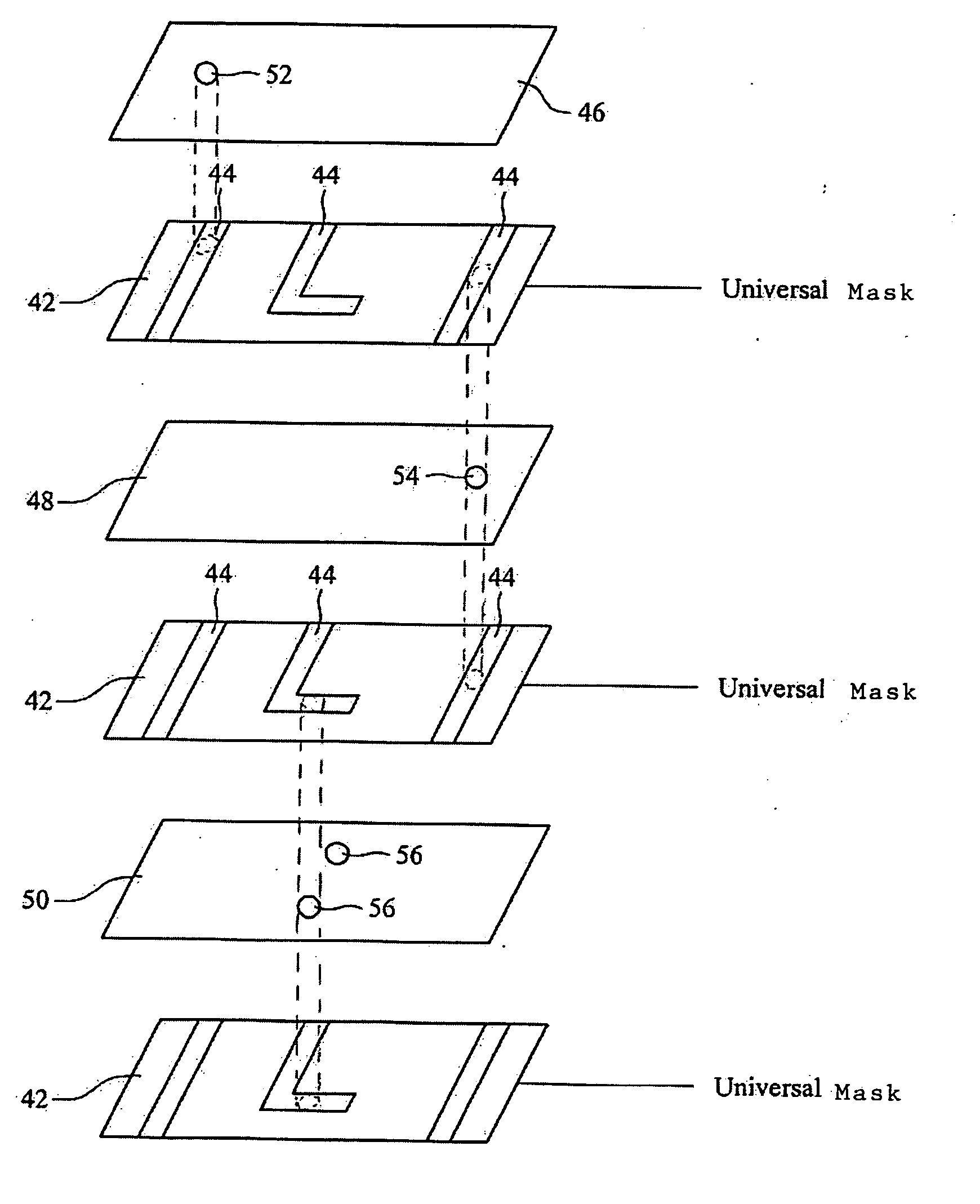
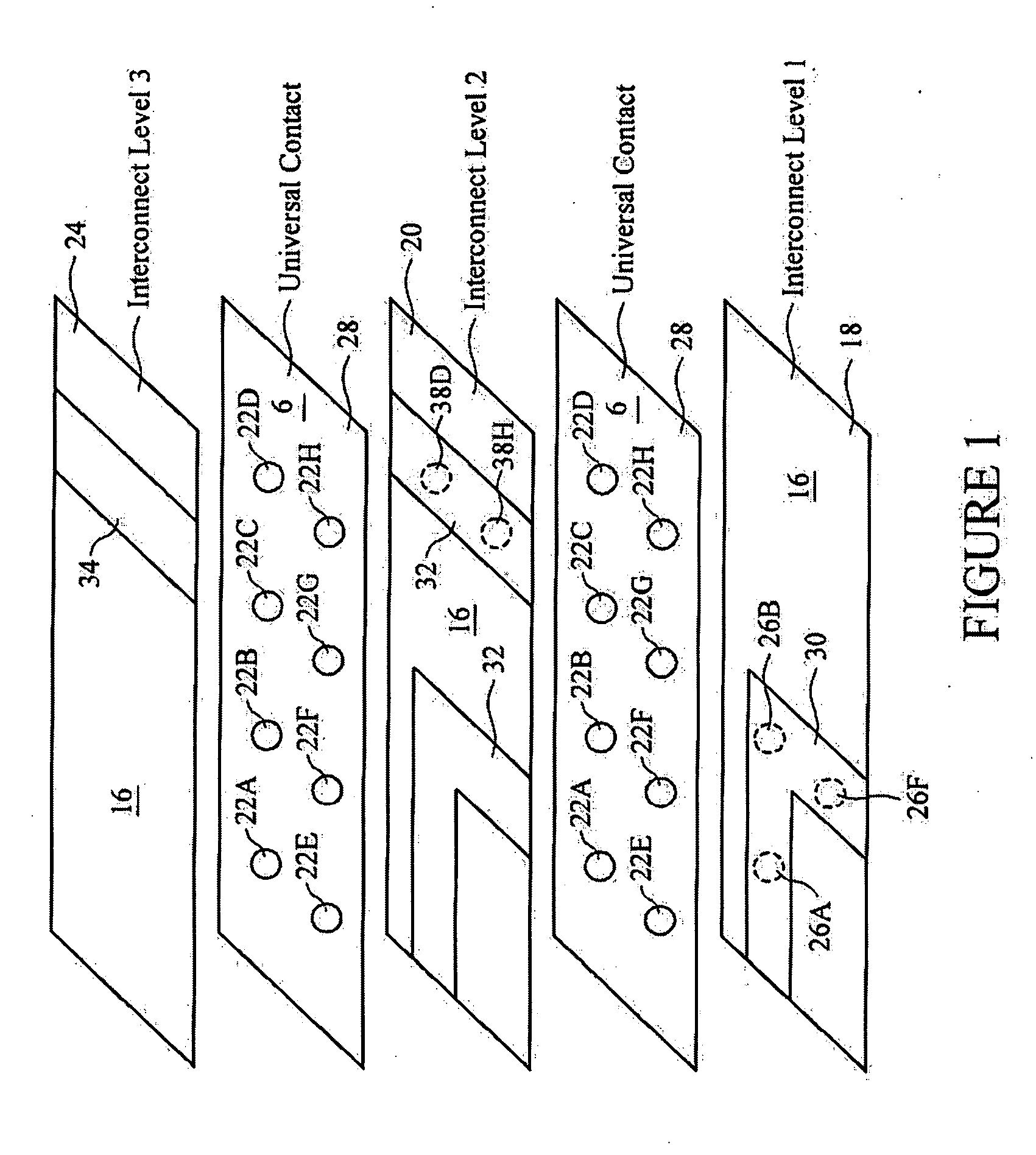
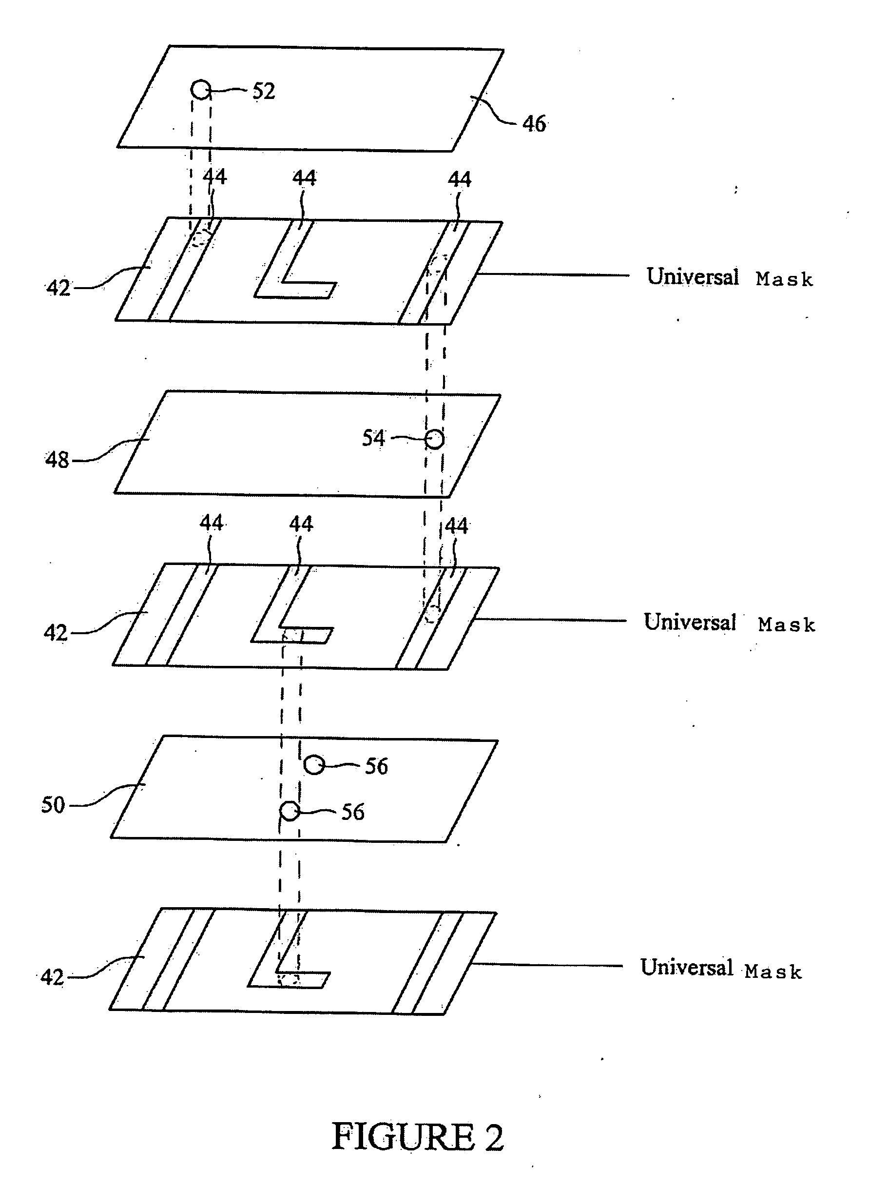
[0014] The invention provides a mask set, also referred to as a photomask set, formed of conventional materials and used to produce a particular semiconductor device. In an exemplary embodiment, the masks are formed using quartz or another transparent material as the substrate and the opaque patterns formed on the mask are formed of chrome or other suitable opaque materials.

[0015] The invention may be used in conjunction with a mask set used in a positive photoresist system, in which the opaque pattern is transferred to a photoresist pattern on the substrate, or with a negative photoresist system, in which the inverse of the opaque pattern is transferred to a photoresist pattern on the substrate as will be transferred to the device. For example, in a positive photoresist system, the interconnect chrome pattern formed on an interconnect level mask is the same as the pattern formed in a photosensitive material on the device and therefore the pattern of the conductive or semiconductiv...


PUM


Abstract

A mask set for forming a semiconductor device includes a universal mask used multiple times in the fabrication process. The universal mask may include contact structures, interconnect structures or both. For each level of use, the universal mask includes some features that provide connection between superjacent and subjacent features and other features that do not provide contact to superjacent or subjacent device features. When used at another level, the other features that did not provide contact between features in the previous location, may advantageously provide contact between superjacent and subjacent structures at the new level. A method for forming a semiconductor device using the described mask set is also provided. The invention further provides a computer program product that provides encoded instructions for forming such a mask set and an apparatus for receiving the instructions and forming the mask set.

Description

FIELD OF THE INVENTION [0001] The present invention relates, most generally, to semiconductor manufacturing and photomask sets used in semiconductor manufacturing. More particularly, the present invention relates to a photomask set with a universal mask, a method for forming the mask set and a method for forming a semiconductor device using the mask set. BACKGROUND [0002] In today's continuously emerging semiconductor manufacturing industry, device cost and manufacturing throughput have been and continue to be salient considerations. Semiconductor devices are manufactured using a coordinated set of photomasks. A photomask is required at each device level. Photomasks must be manufactured to high precision and accuracy standards and therefore the cost of the set of photomasks represents a significant portion of the cost associated with manufacturing the semiconductor device. A complete customized photomask set is required for each particular semiconductor device. For a device having a...

Claims


Application Information

Patent Timeline
IPC IPC(8): G03F9/00G03F1/00
CPCH01L21/76838G03F1/14G03F1/00G03F1/70
Inventor YOO, CHUE SAN
Owner TAIWAN SEMICON MFG CO LTD
Why Eureka
Try Eureka