Method for making a multilayered circuitized substrate

a circuitized substrate and multi-layer technology, applied in the direction of lithographic masks, etching metal masks, conductive pattern formation, etc., can solve the problems of large variation in the quality of thru-holes, large through-holes, and large through-holes, so as to improve the circuitized substrate art

Inactive Publication Date: 2007-08-30
I3 ELECTRONICS
View PDF31 Cites 11 Cited by
  • Summary
  • Abstract
  • Description
  • Claims
  • Application Information

AI Technical Summary

Benefits of technology

[0021] It is, therefore, a primary object of the present invention to enhance the circu

Problems solved by technology

The presence of glass fibers, especially woven glass fibers, also substantially impairs the ability to form high quality, very small thru-holes, including when using a laser.
This problem is increased significantly when patterns of such thru holes are required to satisfy the high density requirements of many of today's circuitized substrates, especially those in the computer field.
This wide variation in encountered glass density leads to problems obtaining the proper laser power for each thru-hole and may result in wide variations in thru-hole quality, obviously unacceptable by today's very demanding manufacturing standards.
The presence of glass fibers in a multilayered structure of the types mentioned herein also often contributes to an electrica

Method used


Image

  • Method for making a multilayered circuitized substrate
  • Method for making a multilayered circuitized substrate
  • Method for making a multilayered circuitized substrate

Examples


Embodiment Construction

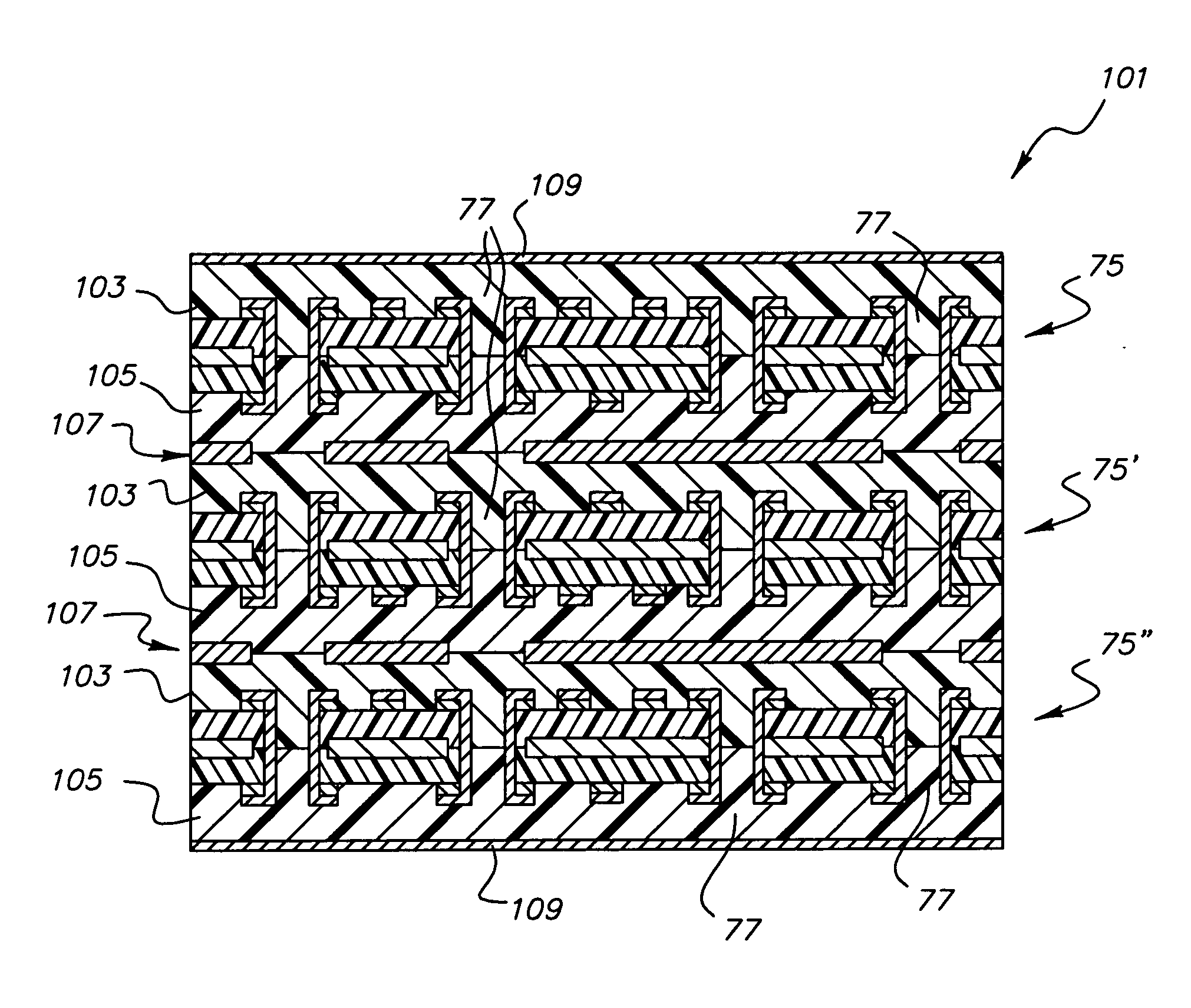
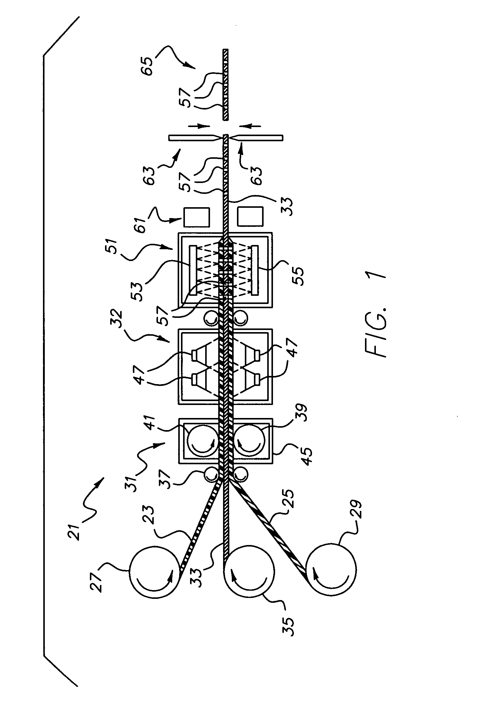
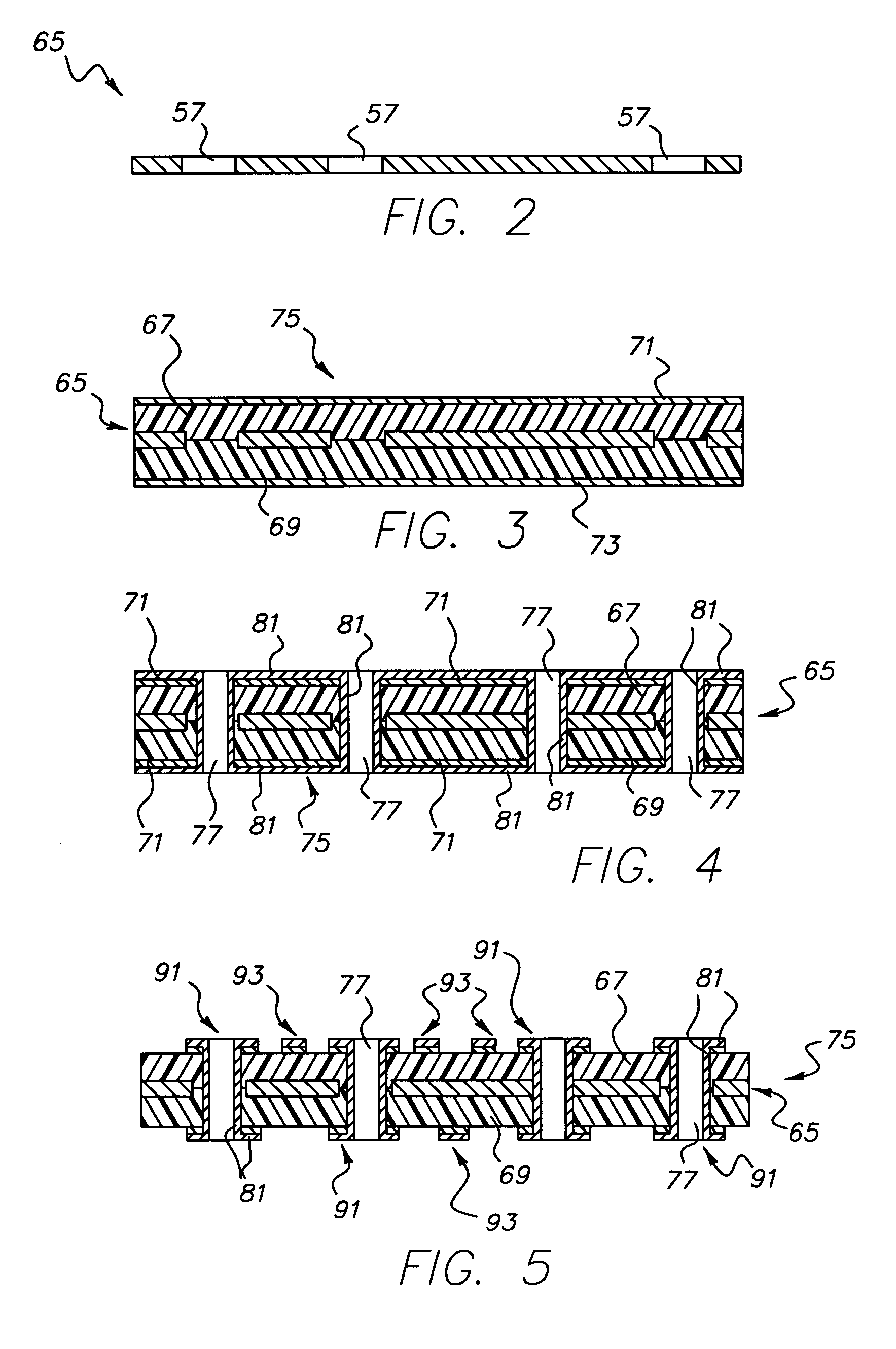
[0027] For a better understanding of the present invention, together with other and further objects, advantages and capabilities thereof, reference is made to the following disclosure and appended claims in connection with the above-described drawings. It is understood that like numerals will be used to indicate like elements from FIG. to FIG.

[0028] By the term “sub-composite” as used herein to define a substrate construction is meant a substrate including at least one dielectric layer and at least one conductive layer bonded thereto, this “sub-composite” adapted for being bonded to other similar sub-composites to form a larger, multilayered circuitized substrate.

[0029] By the term “continuous” as used herein when defining the process to manufacture the conductive layers which will each form an important part of the sub-composites herein is meant that this conductive layer will be in the form of a continuous layer, up to the point of final segmenting thereof to define the layer's ...


PUM

PropertyMeasurementUnit
Temperatureaaaaaaaaaa
Thicknessaaaaaaaaaa
Dielectric polarization enthalpyaaaaaaaaaa

Abstract

A method of making a multilayered circuitized substrate in which a continuous process is used to form electrically conductive layers which each will form part of a sub-composite. The sub-composites are then aligned such that openings within the conductive layers are also aligned, the sub-composites are then bonded together, and a plurality of holes are then laser drilled through the entire thickness of the bonded structure. The dielectric layers used in the sub-composites do not include continuous or semi-continuous fibers therein, thus expediting hole formation there-through,

Description

TECHNICAL FIELD [0001] The present invention relates to the manufacture of multilayered circuitized substrates such as printed circuit boards, chip carriers, and the like. The invention particularly relates to the manufacture of such substrates in which conductive thru-holes are provided therein. CROSS REFERENCE TO CO-PENDING APPLICATIONS [0002] In Ser. No. 11 / 110,919, filed Apr. 21, 2005, there is defined an apparatus and method for making circuitized substrates using a continuous roll format in which layers of conductor and dielectric are fed into the apparatus, bonded, and passed on to other nearby work stations in which various processes such as hole formation, circuitization and, finally, segmentation occur. The resulting substrates can then be individually bonded to other, like substrates to form a larger multi-layered substrate with a plurality of conductive thru-holes, conductive and dielectric layers as part thereof. [0003] In Ser. No. 11 / 110,920, also filed Apr. 21, 2005, ...

Claims


Application Information

Patent Timeline
IPC IPC(8): H05K3/36
CPCH05K3/0032Y10T29/49155H05K3/427H05K3/429H05K3/445H05K3/4623H05K3/4641H05K2201/0355H05K2201/09536H05K2201/096H05K2203/0143H05K2203/0554H05K2203/1545H05K2203/1572Y10T29/49126Y10T29/49165H05K3/0038
Inventor DAVIS, THOMAS J.DESAI, SUBAHU D.LAUFFER, JOHN M.MCNAMARA, JAMES J. JR.MARKOVICH, VOYA R.
Owner I3 ELECTRONICS
Why Eureka
Try Eureka