

Method for determining crystalline orientation using raman spectroscopy
- Summary
- Abstract
- Description
- Claims
- Application Information
AI Technical Summary
Problems solved by technology
Method used
Image

Examples
Embodiment Construction
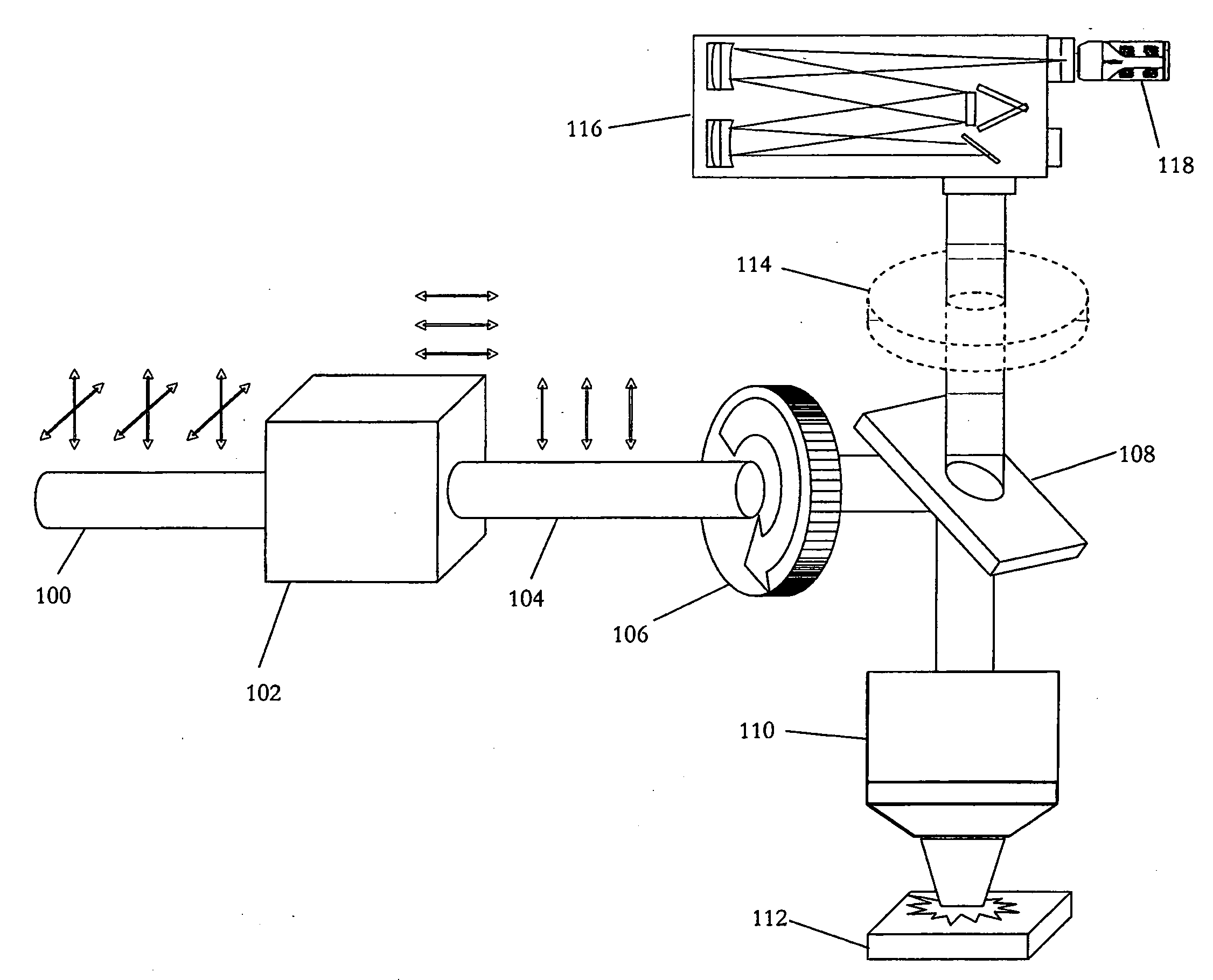
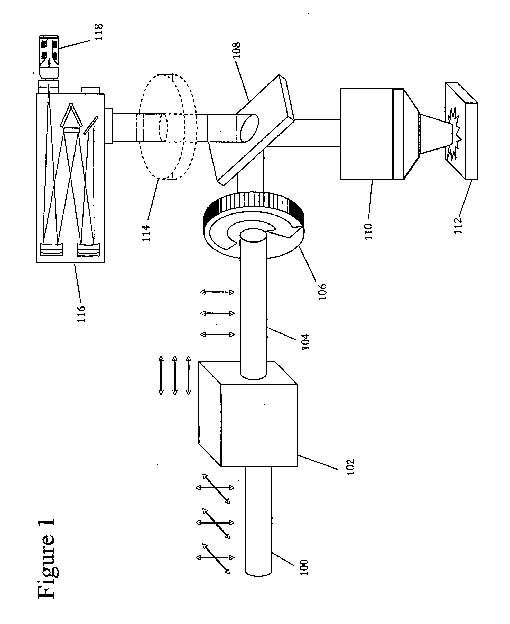
[0028]GaN, because of its excellent material characteristics, is anticipated to replace other materials, such as GaAs, in the manufacture of monolithic microwave integrated circuits (MMIC's). However, it is desirable in these applications to cleave larger, e.g. 2″ diameter, GaN wafers smaller pieces (7.2 mm×7.2 mm) before device fabrication. Identification of crystalline orientation is the first step in the cleaving process. Accurate identification of the crystalline orientation on crystal surfaces is also desirable in other materials and for other semiconductor fabrication processes. Wafer makers typically provide an orientation flat that is used to indicate crystalline orientation. Such flats may have an error of ±0.3° with respect to the actual crystalline orientation. These orientation flats, however, may not be accurate enough for some applications. For example, to obtain good cleaving, the tolerance is desirably about 0.03°.
[0029]FIG. 7 illustrates exemplary coordinate axes th...
PUM
 Abstract
Description
Claims
Application Information