Glass-based micropositioning systems and methods

a micropositioning system and glass-based technology, applied in the field of micropositioning, can solve the problems of increasing device cost, wasting real estate, and difficult use of low-loss coupling to high-index planar waveguide arrays

Inactive Publication Date: 2007-08-30
CORNING INC
View PDF36 Cites 88 Cited by
  • Summary
  • Abstract
  • Description
  • Claims
  • Application Information

AI Technical Summary

Problems solved by technology

Low-loss coupling to high-index planar waveguide arrays can be more difficult using fiber array pigtail blocks, since the smaller mode field diameters (typically 3.5-4.0 μm) are more sensitive to lateral misalignments.
In some cases (e.g., SOA arrays), this pitch requirement can lead to oversized planar device chips and wasted real estate, increasing device cost.
Some planar device substrates (e.g., SOA arrays) are too thin and / or small to make this attachment approach practical.
Control of adhesive flow before thermal or UV curing is also an issue when making attachments to air-clad waveguides and active devices, since sudden cladding index changes can lead to unwanted back reflections and / or scattering.
Since each planar waveguide interconnection requires a separate optical fiber alignment step, the alignment process grows increasingly complex as the number of waveguide interconnections increases.
This has a direct impact on the yield of the assembly and hence, the cost.
Additionally, the fixturing hardware required to hold the fiber in place during attachment (e.g., laser weld clips) generally increases the planar waveguide pitch, further increasing planar device size and cost.
Laser weld attachment methods that require rebending are generally undesirable in planar array interconnection applications, since rebending the optical array interface in the plane of the planar substrate introduces unwanted axial separations between waveguides at one end of the array or the other.
While such systems can generally align waveguide arrays on two planar waveguide devices to within less than 0.2 μm of lateral misalignment, a critical issue is maintaining waveguide alignment during adhesive curing without post-attachment rework.
Crystal block attachment is one solution for zero-shift attachment of devices to substrates, but the cantilever nature of the planar device attachment to the common alignment substrate via an intermediate block makes the approach less suitable for planar devices requiring wirebonded electrical interconnections.
This is a significant disadvantage in micropositioning hybrid optical components because control input must be maintained over the life of the product.
Further, many of the micropositioning technologies described above require complex and expensive precision microstructures (e.g., MEMS) that increase product cost.

Method used


Image

  • Glass-based micropositioning systems and methods
  • Glass-based micropositioning systems and methods
  • Glass-based micropositioning systems and methods

Examples


Embodiment Construction

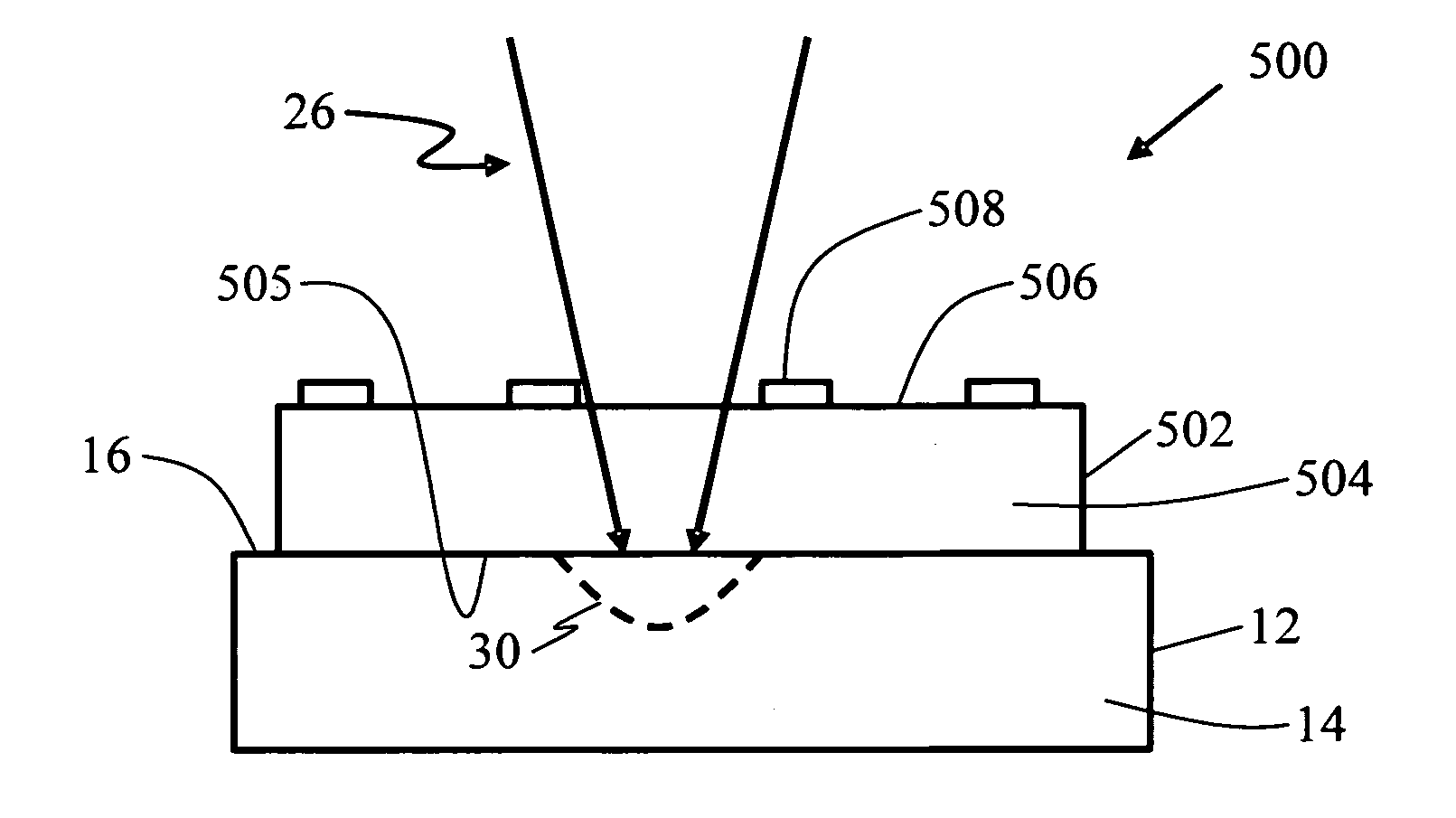
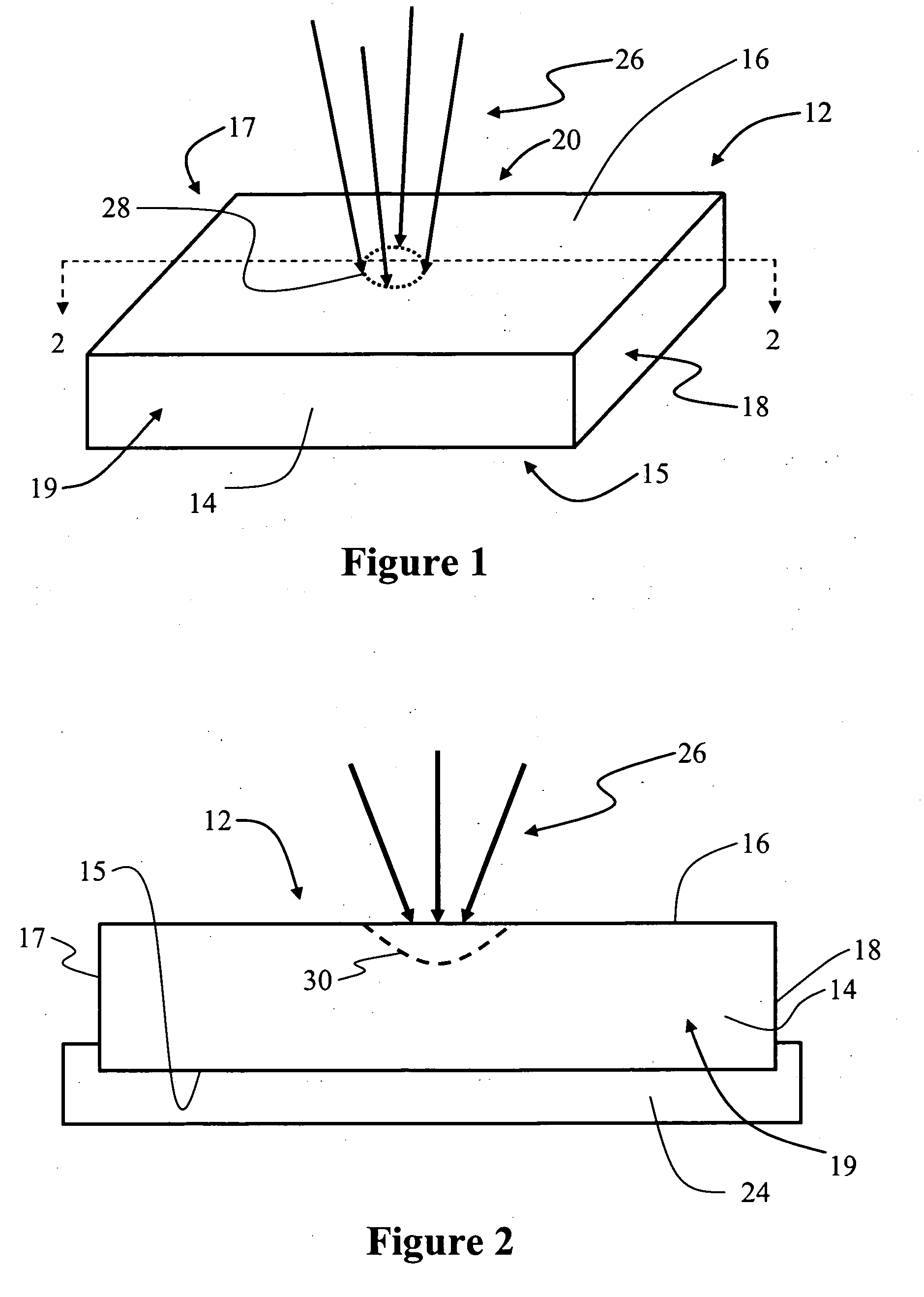
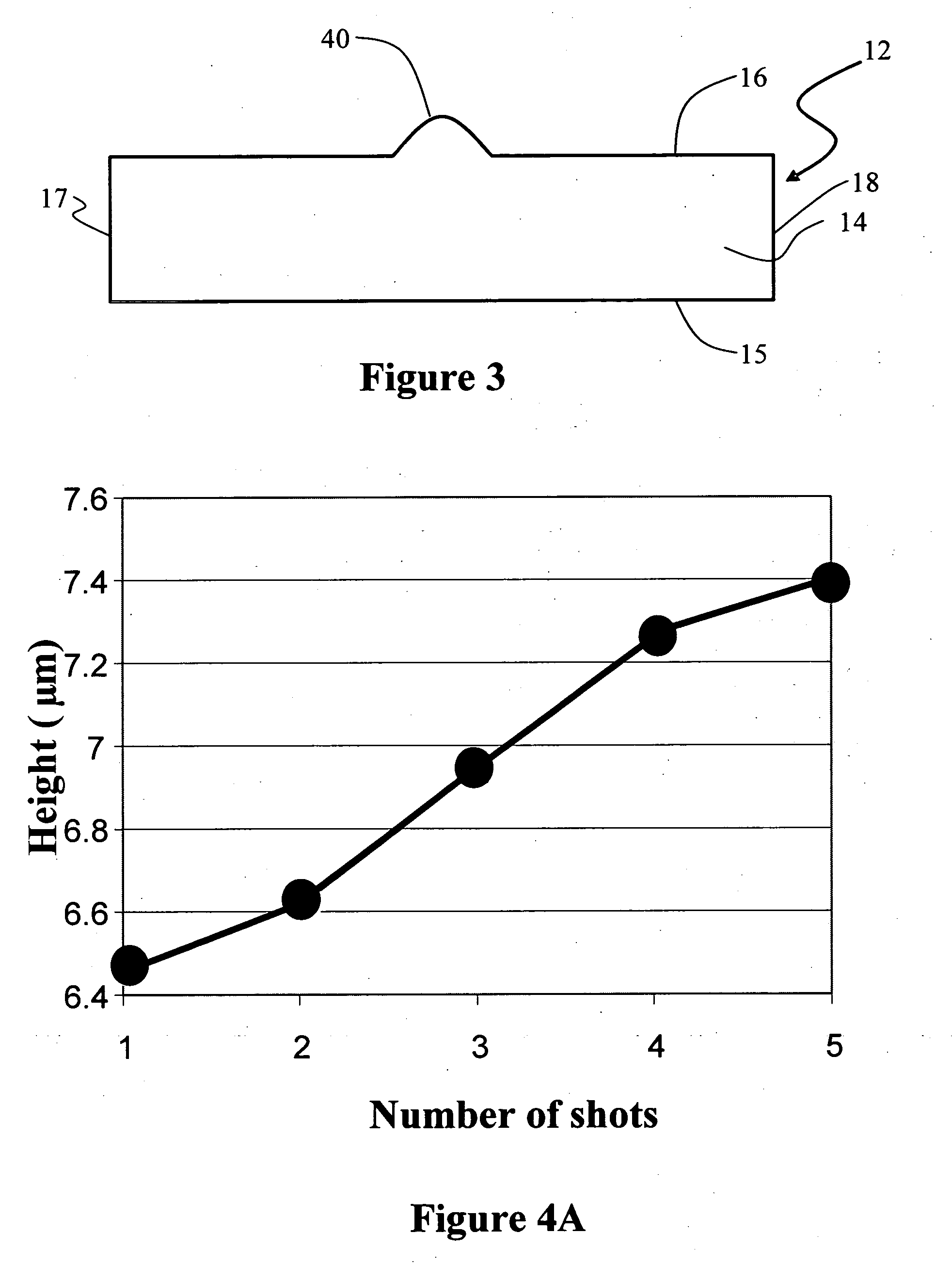
[0054] Reference is now be made in detail to the present preferred embodiments of the invention, examples of which are illustrated in the accompanying drawings. Whenever possible, the same reference numbers and symbols are used throughout the drawings to refer to the same or like parts.

[0055] The present invention includes micropositioning systems and methods that rely on the formation of one or more microbumps in light-absorbing glass substrates. In the description below, various methods of forming microbumps in the light-absorbing substrates are first described. This is followed by a description of example embodiments of methods for micropositioning an optical element via the formation of one or more microbumps in the light-absorbing substrate. An example embodiment of an optical assembly formed using the microbump micropositioning methods of the present invention is then described.

[0056] In the description below, reference is made to PYREX glass, and PYREX is a registered trade...


PUM

PropertyMeasurementUnit
mode field diameteraaaaaaaaaa
diameteraaaaaaaaaa
diameteraaaaaaaaaa

Abstract

Glass-based micropositioning systems and methods are disclosed. The micropositioning systems and methods utilize microbumps (40) formed in a glass substrate (12 or 100). The microbumps are formed by subjecting a portion of the glass substrate to localized heating, which results in local rapid expansion of glass where the heat was applied. The height and shape of the microbumps depend on the type of glass substrate and the amount and form of heat delivered to the substrate. The microbumps allow for active or passive micropositioning of optical elements, including planar waveguides and optical fibers. Optical assemblies formed using microbump micropositioners are also disclosed.

Description

BACKGROUND OF THE INVENTION [0001] 1. Field of the Invention [0002] The present invention relates generally to micropositioning, and particularly to glass-based micropositioning systems and methods. [0003] 2. Technical Background [0004] A micropositioner is a device capable of placing a small object in a desired location and holding it there with a relatively high degree of accuracy and precision. Such positioning is sometimes referred to as either “micropositioning” or “microalignment.” Micropositioners (also referred to as “microactuators”) come in many different forms, such as electromagnetic, mechanical, piezo-electric, micro-electro-mechanical (MEMS), etc., and are used for a wide variety of applications. [0005] Micropositioners are becoming increasingly important in the field of optics, particularly with respect to guided-wave and integrated optics. Planar waveguide technology, for example, enables high-density integration of optical functions, and allows for low-cost fabricat...

Claims


Application Information

Patent Timeline
Patent Type & Authority Applications(United States)
IPC IPC(8): G02B6/42
CPCB29D11/00384G02B6/30G02B6/3636G02B6/3656G02B6/4239G02B6/4227G02B6/423G02B6/4231G02B6/4234G02B6/4226
Inventor GRZYBOWSKI, RICHARD R.HEMENWAY, BREWSTER ROE JR.HUGHES, LAWRENCE CHARLES JR.LOGUNOV, STEPHAN LVOVICHREDDY, KAMJULA PATTABHIRAMISCHROEDER, JOSEPH FRANCIS IIISUTHERLAND, JAMES SCOTT
Owner CORNING INC
Why Eureka
Try Eureka