Mixed-scale electronic interface

a technology of electronic interface and mixed-scale, applied in the direction of electrical equipment, semiconductor devices, instruments, etc., can solve the problems of high cost, design and fabrication overhead, and inability to meet the needs of mixing-scale microelectronic devices, and achieve the effect of improving reliability, cost and reliability

Inactive Publication Date: 2007-09-06
HEWLETT-PACKARD ENTERPRISE DEV LP
View PDF3 Cites 47 Cited by
  • Summary
  • Abstract
  • Description
  • Claims
  • Application Information

AI Technical Summary

Problems solved by technology

In many cases, devising reliable and cost-effective interfaces between microscale and submicroscale electronics and nanoscale electronics has proven to be more difficult than the design and fabrication of nanoscale electronic devices.
Demultiplexer-based nanoscale / microscale interfaces may therefore represent significant bandwidth bottlenecks within mixed-scale microelectronic devices.
The demultiplexer-based approach may additionally add design and fabrication overheads, cost, and reliability problems to mixed-scale electronic devices with densely interconnected microscale and nanoscale circuits and functional modules.

Method used


Image

  • Mixed-scale electronic interface
  • Mixed-scale electronic interface
  • Mixed-scale electronic interface

Examples


Embodiment Construction

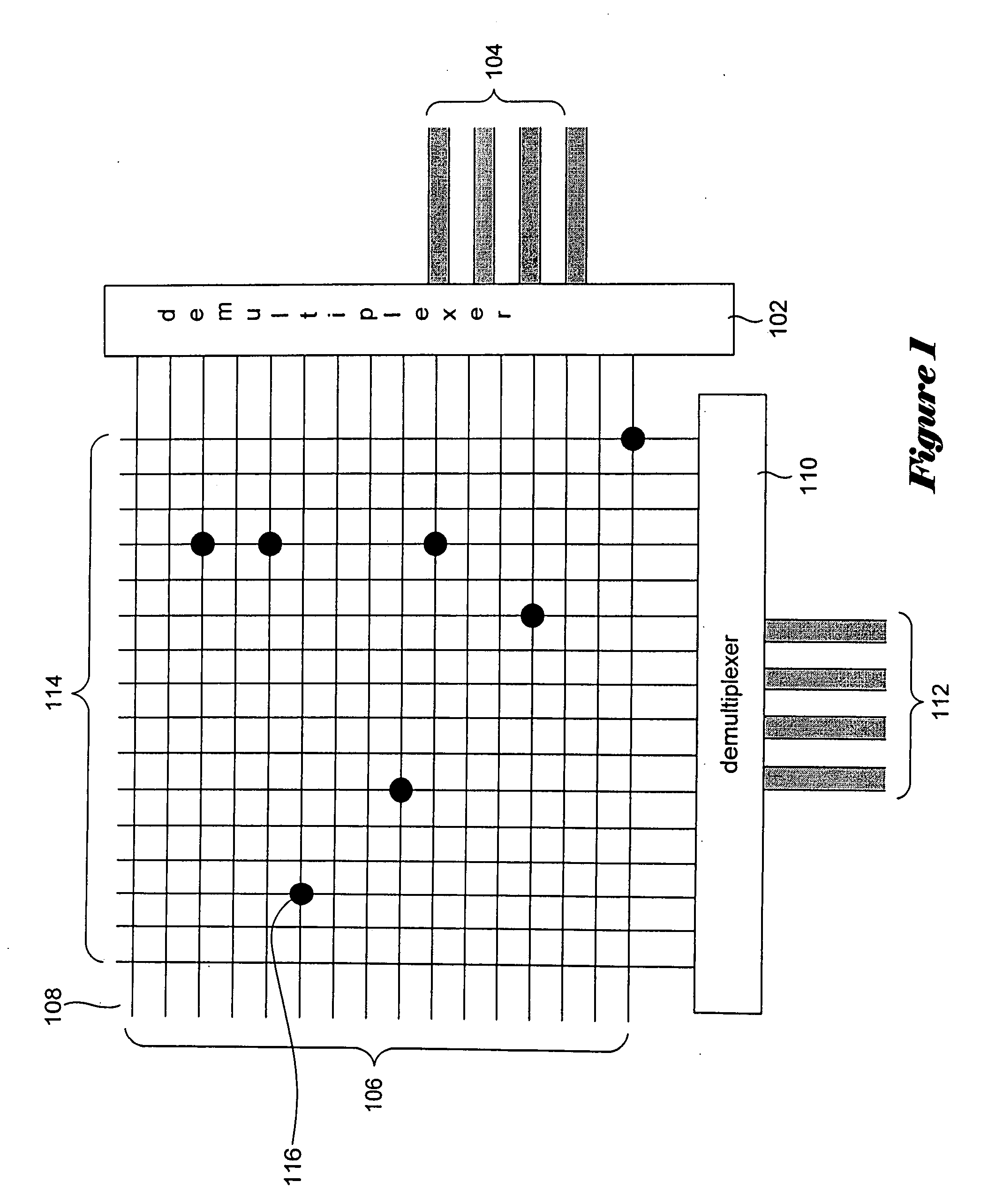
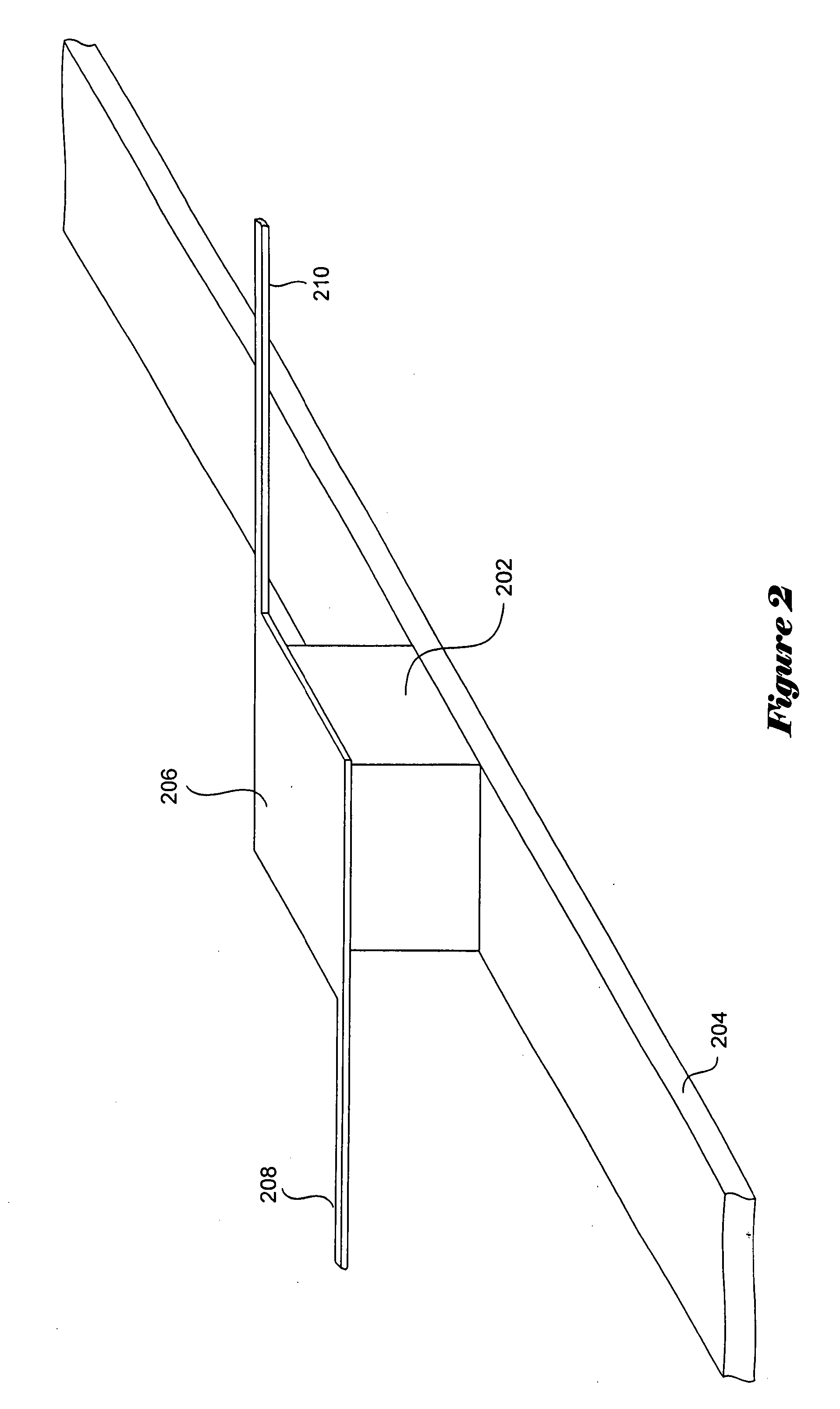
[0029] Embodiments of the present invention are directed to nanoscale / microscale interfaces that permit dense interconnections between microscale and submicroscale features and logic and nanoscale features and logic within an integrated circuit or other electronic device. In the current discussion, the term “nanoscale” refers to features and components with a least one dimension smaller than 100 nanometers. Alternatively, the term “nanoscale” may refer to features and components with at least one dimension smaller than 50 nanometers, and, in certain cases, less than 10 nanometers. The term “submicroscale” generally refers to features and components with at least on dimension smaller than 1 micron, and the term “microscale” refers to features and components with dimensions equal to, or greater than, 1 micron. In general, microscale and submicroscale features and components can be fabricated by conventional photolithographic techniques, but nanoscale components and features can genera...


PUM


Abstract

Embodiments of the present invention are directed to mixed-scale electronic interfaces, included in integrated circuits and other electronic devices, that provide for dense electrical interconnection between microscale features of a predominantly microscale or submicroscale layer and nanoscale features of a predominantly nanoscale layer. The predominantly nanoscale layer, in one embodiment of the present invention, comprises a tessellated pattern of submicroscale or microscale pads densely interconnected by nanowire junctions between sets of parallel, closely spaced nanowire bundles. The predominantly submicroscale or microscale layer includes pins positioned complementarily to the submicroscale or microscale pads in the predominantly nanoscale layer. Pins can be configured according to any periodic tiling of the microscale layer.

Description

CROSS-REFERENCE TO RELATED APPLICATION [0001] This application is a continuation-in-part to U.S. application Ser. No. 11 / 342,076, filed Jan. 27, 2006.TECHNICAL FIELD [0002] The present invention is related to integrated circuits and other electronic devices and, in particular, to a mixed-scale interface suitable for densely interconnecting nanoscale electronics with microscale electronics within an integrated circuit or other electronic device. BACKGROUND OF THE INVENTION [0003] As manufacturers and designers of integrated circuits continue to relentlessly decrease the size of integrated-circuit features, such as transistors and signal lines, and to correspondingly increase the density at which features can be fabricated within integrated circuits, they are beginning to approach fundamental physical limits to further decreases in feature sizes for integrated circuits fabricated by conventional photolithography techniques. Research efforts have, during the past decade, turned to new,...

Claims


Application Information

Patent Timeline
Patent Type & Authority Applications(United States)
IPC IPC(8): H01L29/00
CPCB82Y10/00G11C2213/81H01H1/0094H01L27/285H01L51/0595H01L29/0673H01L29/0676H01L51/0591H01L29/0665H10K19/202H10K10/50H10K10/701H01L21/82B82Y40/00
Inventor WILLIAMS, R. STANLEYSNIDER, GREGORY S.STEWART, DUNCAN
Owner HEWLETT-PACKARD ENTERPRISE DEV LP
Why Eureka
Try Eureka