Cover tape for packaging semiconductor device and package for semiconductor device
- Summary
- Abstract
- Description
- Claims
- Application Information
AI Technical Summary
Benefits of technology
Problems solved by technology
Method used
Image
Examples
first embodiment
[0032]The first embodiment of the cover tape for packaging semiconductor device of the present invention will be explained referring to figures below.
[0033]FIG. 2A is a perspective view showing the cover tape for packaging semiconductor device of the present invention in the first embodiment.
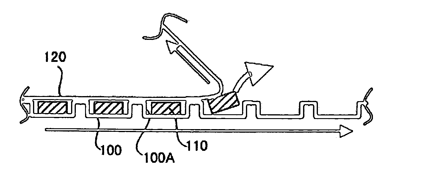
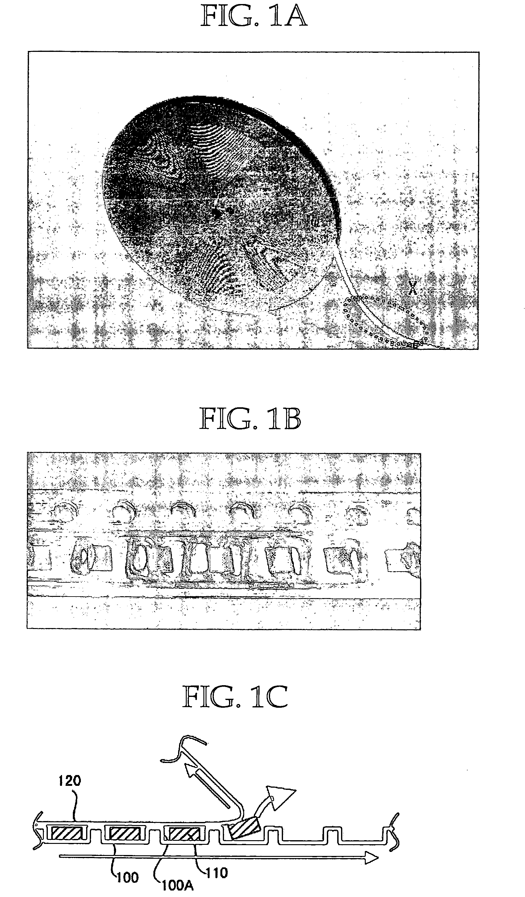
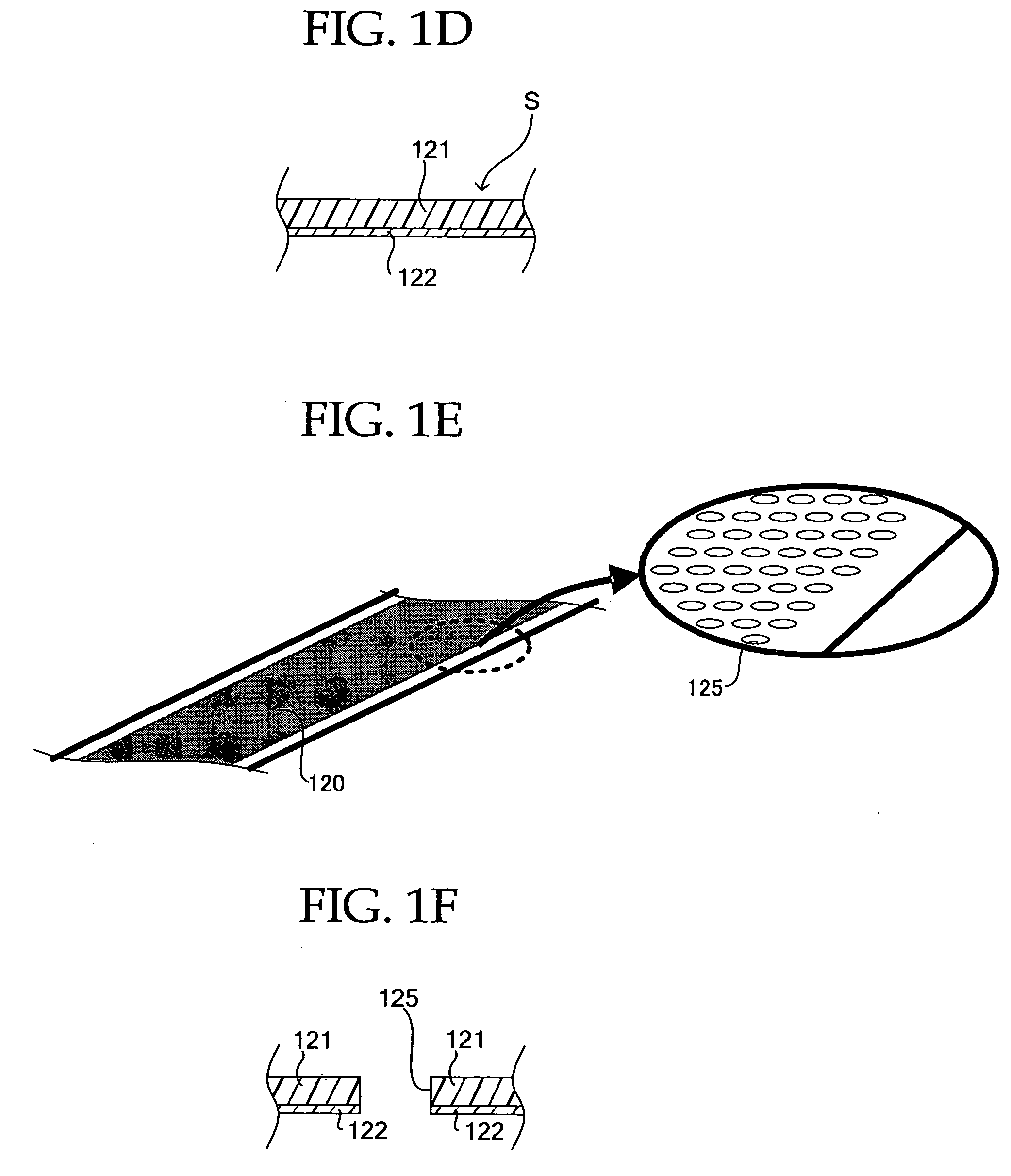
[0034]A cover tape 10 as shown in FIG. 2A is pasted on the embossed tape for use. The embossed tape is not particularly limited and may be selected from known embossed tapes accordingly. Examples include an embossed tape 100 as shown in FIG. 1C on which pockets (concave portions) 100A are formed at regular intervals in a length direction for containing semiconductor devices (IC chips 110, for example). The cover tape 10 prevents dropout of semiconductor devices (IC chips 110, for example) contained in the pockets 100A on the embossed tape 100 when pasted on the embossed tape 100. Furthermore, the cover tape 10 is shipped and transported as wound on reels with the embossed tape 100 (FIG. 1A). The...
PUM
 Abstract
Description
Claims
Application Information
 - R&D
- Intellectual Property
- Life Sciences
- Materials
- Tech Scout
- Unparalleled Data Quality
- Higher Quality Content
- 60% Fewer Hallucinations
Browse by: Latest US Patents, China's latest patents, Technical Efficacy Thesaurus, Application Domain, Technology Topic, Popular Technical Reports.
© 2025 PatSnap. All rights reserved.Legal|Privacy policy|Modern Slavery Act Transparency Statement|Sitemap|About US| Contact US: help@patsnap.com


